Structure and method for manufacturing MOSFET with super-steep retrograded island

a technology of retrograded island and mosfet, which is applied in the direction of transistors, semiconductor devices, electrical equipment, etc., can solve the problems of reducing gate control, reducing mobility, and reducing the subthreshold characteristics of devices, so as to reduce the incidence of short-channel effects

Inactive Publication Date: 2006-03-30
GLOBALFOUNDRIES INC
View PDF3 Cites 141 Cited by
  • Summary
  • Abstract
  • Description
  • Claims
  • Application Information

AI Technical Summary

Benefits of technology

[0007] One object of the present invention is to provide a MOSFET device, and a method of forming thereof, having a steep retrograded dopant island, in which the steep retrograded dopant island is located underlying the device channel and effectively reduces the incidence of short-channel effects. It is another object of the present invention to provide a steep retrograded dopant island that is substantially aligned to the sidewalls of the overlying gate region. It is a further object of the present invention to integrate the steep retrograded dopant island with strained-Si device improvements. The term “steep retrograded dopant island” denotes a doped region underlying the device channel of a MOSFET, in which the edge of the dopant region is substantially aligned to the sidewalls of the overlying gate region.

Problems solved by technology

This results in a degradation of the subthreshold characteristics of the device and a failure to achieve current saturation, which ultimately reduces control of the gate.
One can suppress the short-channel effect by highly doping the channel, at the expense of reduced mobility, lower operating speed and increased risk for avalanches at the drain.
The high concentration of counter-dopant at the PN junctions (source / channel interface, channel / drain interface) of the device disadvantageously result in increased device leakage.

Method used


Image

  • Structure and method for manufacturing MOSFET with super-steep retrograded island
  • Structure and method for manufacturing MOSFET with super-steep retrograded island
  • Structure and method for manufacturing MOSFET with super-steep retrograded island

Examples


Embodiment Construction

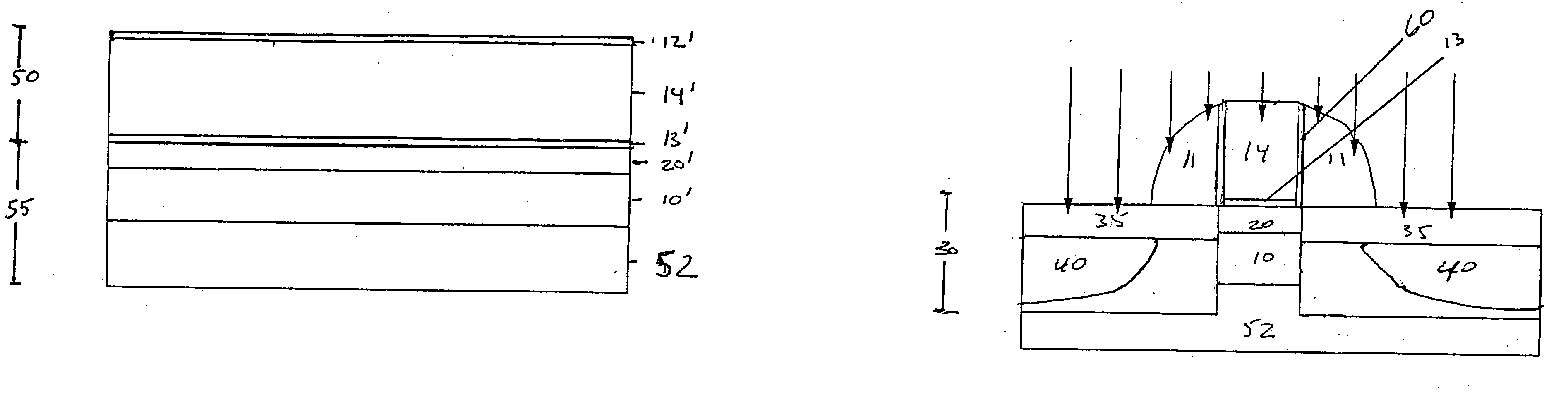
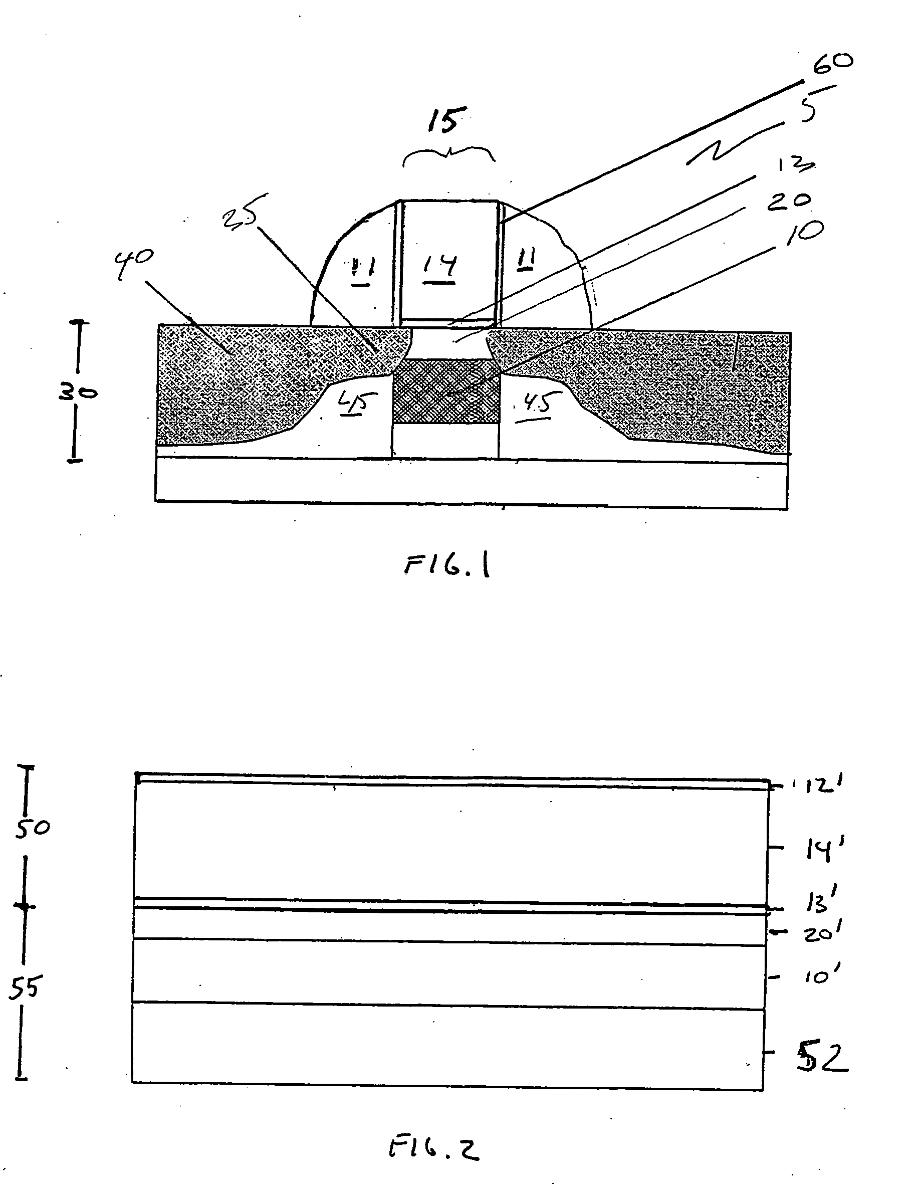
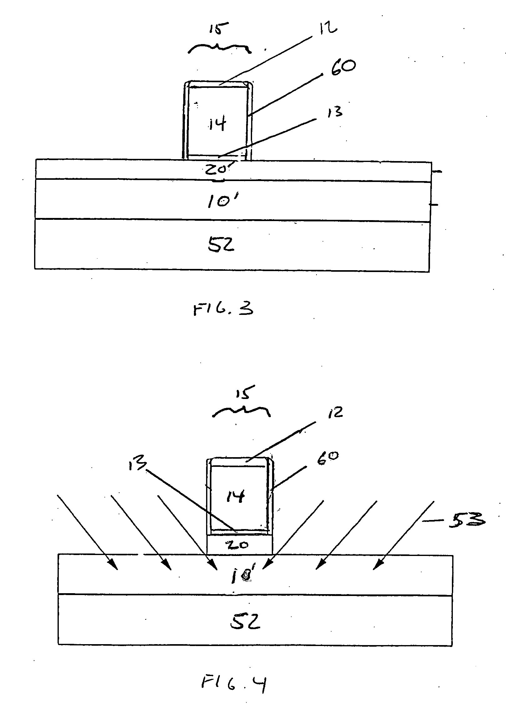
[0028] The present invention, which is directed to a MOSFET having a steep retrograded dopant island that reduces short-channel effects without increasing device leakage, and a method of forming a MOSFET having a steep retrograded dopant island, will now be discussed in greater detail by referring to the drawings that accompany the present application. In the accompanying drawings, like and or corresponding elements are referred to by like reference numbers.

[0029] Referring to FIG. 1, illustrating one embodiment of the present invention, a MOSFET 5 is provided comprising a steep retrograded dopant island 10, in which the steep retrograded dopant island 10 is substantially aligned with the sidewalls of the overlying gate region 15. The gate region 15 includes a gate conductor 14, and a gate dielectric 13. Sidewall spacers 60 and offset spacers 11 are positioned adjacent to the gate region 15. The steep retrograded dopant island 10 comprises a first conductivity type dopant in a conc...


PUM


Abstract

The present invention comprises a method for forming a semiconducting device including the steps of providing a layered structure including a substrate, a low diffusivity layer of a first-conductivity dopant; and a channel layer; forming a gate stack atop a protected surface of the channel layer; etching the layered structure selective to the gate stack to expose a surface of the substrate, where a remaining portion of the low diffusivity layer provides a retrograded island substantially aligned to the gate stack having a first dopant concentration to reduce short-channel effects without increasing leakage; growing a Si-containing material atop the recessed surface of the substrate; and doping the Si-containing material with a second-conductivity dopant at a second dopant concentration. The low diffusivity layer may be Si1-x-yGexZy, where Z can be carbon (C), xenon (Xe), germanium (Ge), krypton (Kr), argon (Ar), nitrogen (N), or combinations thereof.

Description

FIELD OF THE INVENTION [0001] The present invention relates to semiconductor devices and methods of manufacture, and more particularly to a method for manufacturing an improved metal oxide semiconductor (MOS) transistor having a steep retrograded dopant island. BACKGROUND OF THE INVENTION [0002] Field effect transistors (FETs) are the basic building block of today's integrated circuits (ICs). Such transistors can be formed in conventional bulk semiconductor substrates (such as silicon) or in an SOI layer of a silicon-on-insulator (SOI) substrate. [0003] In order to be able to make ICs, such as memory, logic, and other devices, of higher integration density than currently feasible, one has to find ways to further downscale the dimensions of field effect transistors (FETs), such as metal-oxide-semiconductor field effect transistors (MOSFETs) and complementary metal oxide semiconductors (CMOS). Scaling achieves compactness and improves operating performance in devices by shrinking the ...

Claims


Application Information

Patent Timeline
Patent Type & Authority Applications(United States)
IPC IPC(8): H01L21/336
CPCH01L21/26586H01L21/823807H01L21/823814H01L29/105H01L29/1608H01L29/7848H01L29/6659H01L29/66636H01L29/7833H01L29/7842H01L29/6656
Inventor ZHU, HUILONGLEOBANDUNG, EFFENDIMOCUTA, ANDA C.MOCUTA, DAN M.
Owner GLOBALFOUNDRIES INC
Why Eureka
Try Eureka