Semiconductor device having a gate insulating film structure including an insulating film containing metal, silicon and oxygen and manufacturing method thereof

a technology of insulating film and semiconductor device, which is applied in the direction of semiconductor device, electrical apparatus, transistor, etc., can solve the problems of difficult to obtain good interface, and difficult to achieve the best combination of metal oxide film and metal silicate film, etc., to achieve the effect of enhancing the productivity of manufacturing miniature semiconductor devi

Inactive Publication Date: 2007-12-11
HEAD TECHNOLOGY GMBH LTD +1
View PDF18 Cites 17 Cited by
  • Summary
  • Abstract
  • Description
  • Claims
  • Application Information

AI Technical Summary

Benefits of technology

[0013]Accordingly, the object of the present invention is to solve these problems by providing a semiconductor device having a metal oxide film or an insulating film containing metal, silicon and oxygen. Specifically, the present invention provides a metal silicate film as a gate insulating film where the characteristics of the elements in a semiconductor device and the productivity of manufacturing miniature semiconductor device are enhanced and its manufacturing method thereof.SUMMARY OF THE INVENTION
[0015]According to the object of the present invention, the dangling bond on the interface between the metal silicate film and silicon that made up the semiconductor substrate can be brought to an end by fluorine contained in the metal silicate film. Therefore, the interface state density can be lowered as compared to a metal silicate film without fluorine and a good interface characteristic is attained.
[0016]Further, the dielectric constant of the metal silicate film is increased and the effective film thickness reduced when it contains nitrogen. The annealing process for the metal oxide film is carried out under an oxidizing atmosphere (to compensate for oxygen deficiency) to avert the oxidizing reaction in the interface between the metal silicate film and silicon which made up the semiconductor substrate. Thus, the effective film thickness is reduced and good interfacial characteristic such as a low interface state density is attained.
[0017]Thus, a high performance transistor is produced by positioning a metal-containing metal silicate insulating film, having silicon, oxygen, and at least one fluorine and one nitrogen between the semiconductor substrate and the metal oxide film. The transistor thus produced has a good interfacial characteristic with a film gate insulating film containing metal silicate film that has a reduced effective film thickness and a reduced leak current.
[0018]A semiconductor device according to another aspect of the present invention has a gate insulating film constructed by laminating a metal silicate insulating film having metal, silicon, and oxygen together with an amorphous metal oxide film. The gate insulating film having the metal oxide film and metal silicate film thus produced has a reduced effective film thickness and a reduced leak current. Further, since the metal oxide film is an amorphous film, a transistor thus produced has a reduced variation of the effective film thickness which depends on the dielectric constant of the crystal plan orientation and a less variation in the threshold voltage with excellent reliability.

Problems solved by technology

However, when the metal oxide film is used as the gate insulating film, it is difficult to obtain a good interface which is free from distortion in a portion facing a silicon substrate.
Additionally, when the metal silicate film is used as the gate insulating film, a mediocre interface is attained, with a smaller dielectric constant than that of the metal oxide film.
Unfortunately, with time, the constituent metals of the two films become the same.
Therefore, it is difficult to attain the best combination of the metal oxide film and metal silicate film by using different kinds of the constituent metals of the two films.
Unfortunately, this process is complicated and inefficient.
However, there are many problems in maintaining the characteristics of the gate insulating film while attaining the reduction in the physical and / or the actual film thickness.
Specifically, problems with respect to the characteristic of the resulting elements and the productivity of manufacturing the elements.

Method used


Image

  • Semiconductor device having a gate insulating film structure including an insulating film containing metal, silicon and oxygen and manufacturing method thereof
  • Semiconductor device having a gate insulating film structure including an insulating film containing metal, silicon and oxygen and manufacturing method thereof
  • Semiconductor device having a gate insulating film structure including an insulating film containing metal, silicon and oxygen and manufacturing method thereof

Examples


embodiment 1

[0042]Without wishing to unnecessarily limit the foregoing, the following shall discuss the invention with respect to certain preferred embodiments.

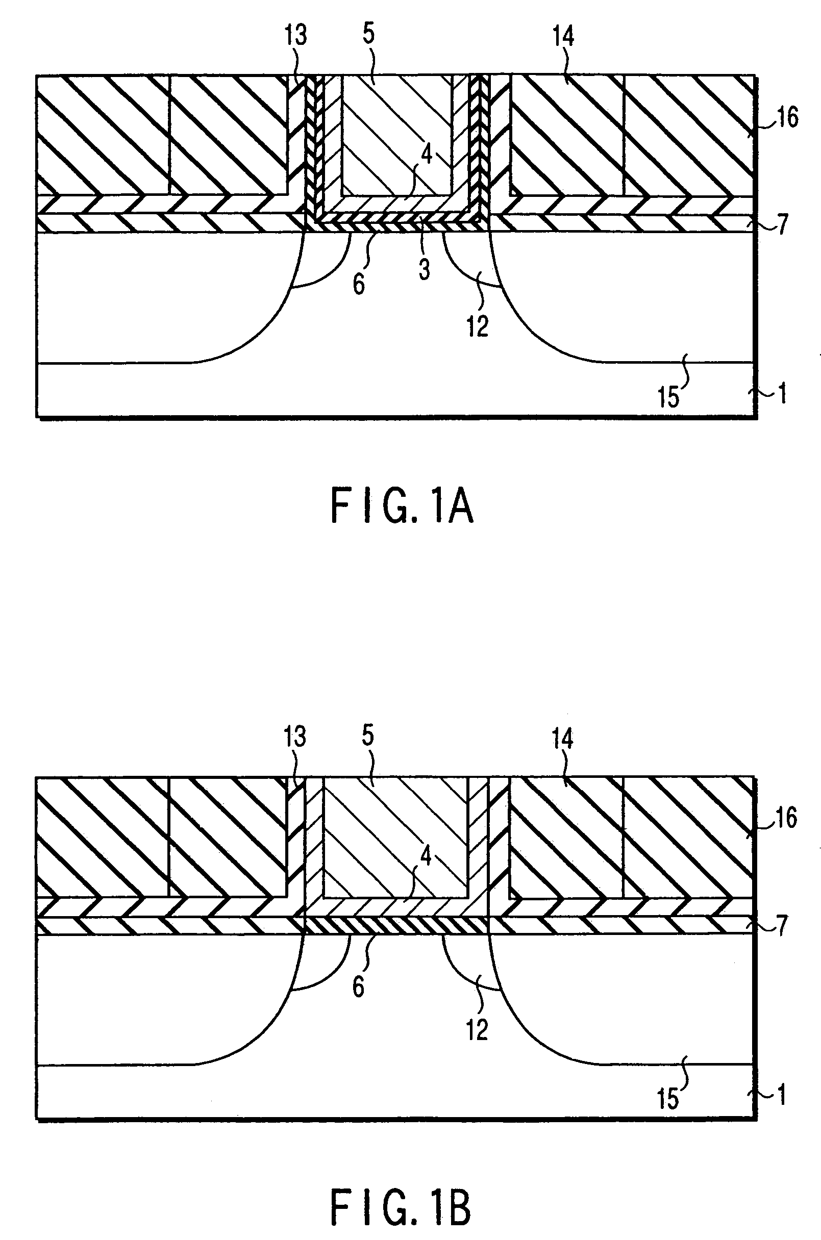
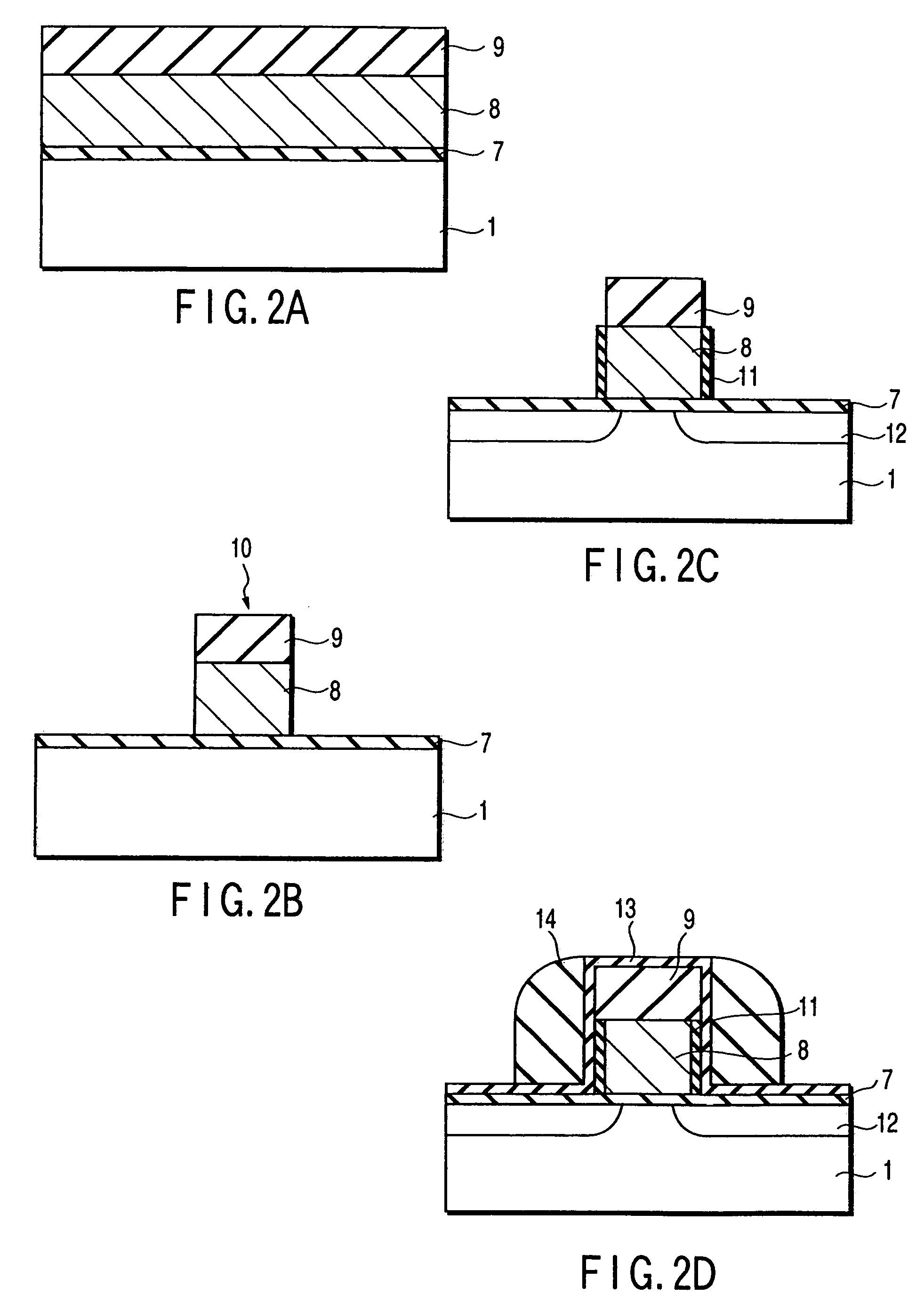
[0043]A first embodiment of this invention will now be described with reference to FIGS. 1A to 1B and 2A to 2I of the accompanying drawings.

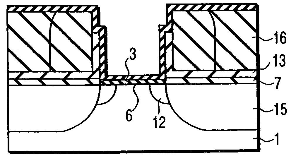
[0044]FIG. 1A shows a structure of a semiconductor device according to the first embodiment of this invention.

[0045]A metal silicon-oxygen material film (hereinafter a “metal silicate film”) 6 (which is a zirconium silicate film in accordance with this embodiment) as a compound of metal, silicon and oxygen, and a metal oxide film 3 (which is a zirconium oxide film in accordance with this embodiment) are formed as a gate insulating film on a silicon substrate 1. A titanium nitride film 4 is formed on metal oxide film 3 and a tungsten film 5 is formed on titanium nitride film 4 so as to fill a cavity formed on titanium nitride film 4 so that a multi-layered gate electrode is formed on metal oxide film ...

embodiment 2

[0070]FIG. 3 is a cross sectional view of a semiconductor device according to a second embodiment of this invention. The basic structure is similar to that of the embodiment 1 shown in FIG. 1A and portions of FIG. 3 which corresponds to those of FIG. 1A are denoted by the same reference numerals.

[0071]In the embodiment shown in FIG. 3, a zirconium silicate film 6 is formed only on the surface of a substrate 1, the film thickness thereof is approximately 1.5 nm, the film thickness of a zirconium oxide film 3 is approximately 3 nm, the film thickness obtained by converting the film thickness of each of these films into the film thickness of a silicon oxide film is approximately 0.5 nm and the total effective gate insulating film thickness is approximately 1 nm. In this embodiment, a small amount of nitrogen instead of fluorine is contained in zirconium silicate film 6 between the gate electrode and silicon substrate 1. The width of the gate electrode is approximately 50 nm.

[0072]It is...

embodiment 3

[0091]The structure and manufacturing process of a semiconductor device according to an embodiment 3 of this invention will now be explained. The basic structure is similar to that of embodiment 2 shown in FIG. 3, except that the constituent material of the gate insulating film is amorphous. Embodiment 3 will now be explained with reference to FIG. 3.

[0092]Like embodiment 2, embodiment 3 uses zirconium oxide film as a metal oxide film 3 and a zirconium silicate film as a metal silicate film 6. The film thickness of zirconium silicate film 6 is approximately 1.5 nm, the film thickness of zirconium oxide film 3 is approximately 3 nm, the film thickness obtained by converting the film thickness of each of the above films 3 and 6 into the film thickness of a silicon oxide film is approximately 0.5 nm and the effective gate insulating film thickness is approximately 1 nm. The width of the gate electrode is approximately 50 nm.

[0093]Similar to embodiment 2, it is possible to use various t...


PUM

PropertyMeasurementUnit
thicknessaaaaaaaaaa
thicknessaaaaaaaaaa
thicknessaaaaaaaaaa

Abstract

Claimed and disclosed is a semiconductor device including a transistor having a gate insulating film structure containing nitrogen or fluorine in a compound, such as metal silicate, containing metal, silicon and oxygen, a gate insulating film structure having a laminated structure of an amorphous metal oxide film and metal silicate film, or a gate insulating film structure having a first gate insulating film including an oxide film of a first metal element and a second gate insulating film including a metal silicate film of a second metal element.

Description

[0001]This application is a divisional of U.S. patent application Ser. No. 09 / 803,265, filed Mar. 9, 2001, now U.S. Pat. No. 6,784,508 the entire contents of which are incorporated herein by reference, and which is based upon and claims priority to Japanese Application No. 2000-066960 filed Mar. 10, 2000, incorporated herein by reference.RELATED APPLICATION[0002]This application claims priority to Japanese Application No. 2000-066960 filed Mar. 10, 2000, incorporated herein by reference.BACKGROUND OF THE INVENTION[0003]1. Field of the Invention[0004]This invention is directed to a semiconductor device and a manufacturing method of the semiconductor device. More particularly to a semiconductor device having a gate insulating film structure including an insulating film which contains metal, silicon and oxygen, for example, a metal silicate film and the manufacturing method thereof.[0005]2. Description of the Related Art[0006]It is desirable to make a thin gate insulating film for the ...

Claims


Application Information

Patent Timeline
Patent Type & Authority Patents(United States)
IPC IPC(8): H01L21/8234H01L21/283H01L21/28H01L21/316H01L21/336H01L29/49H01L29/51H01L29/78
CPCH01L21/28088H01L29/6656H01L21/28194H01L21/28202H01L21/28211H01L21/82345H01L21/823462H01L21/823475H01L29/4966H01L29/513H01L29/517H01L29/518H01L29/66545H01L21/28185H01L21/31604H01L21/02271H01L21/02189H01L21/022H01L21/02159H01L21/18
Inventor TSUNASHIMA, YOSHITAKAINUMIYA, SEIJISUIZU, YASUMASAOZAWA, YOSHIOMIYANO, KIYOTAKATANAKA, MASAYUKI
Owner HEAD TECHNOLOGY GMBH LTD
Why Eureka
Try Eureka