Novel composite structure full back-side heterojunction solar cell and preparation method thereof

A composite structure and solar cell technology, applied in circuits, photovoltaic power generation, electrical components, etc., can solve problems such as poor workmanship, scratches that reduce battery efficiency, and abnormal leakage, so as to ensure the life of minority carriers and reduce the recombination current density. , Improve the effect of short-circuit current density

Active Publication Date: 2018-12-07
拉普拉斯新能源科技股份有限公司
View PDF5 Cites 15 Cited by
  • Summary
  • Abstract
  • Description
  • Claims
  • Application Information

AI Technical Summary

Problems solved by technology

[0004] 1) When the silicon wafer is placed on the positioning card point, it is inevitable to rub and cause scratches and reduce battery efficiency;
[0005] 2) Due to the inclination of the silicon wafer, the gap between the back of the silicon wafer and the graphite plate is relatively large, which can easily cause the phenomenon of winding plating and reduce the efficiency of the battery, and even cause abnormal

Method used


Image

  • Novel composite structure full back-side heterojunction solar cell and preparation method thereof
  • Novel composite structure full back-side heterojunction solar cell and preparation method thereof
  • Novel composite structure full back-side heterojunction solar cell and preparation method thereof

Examples


Embodiment Construction

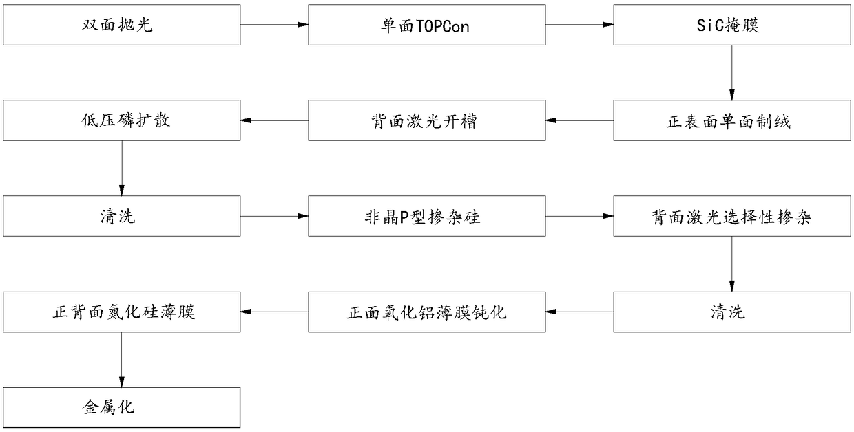
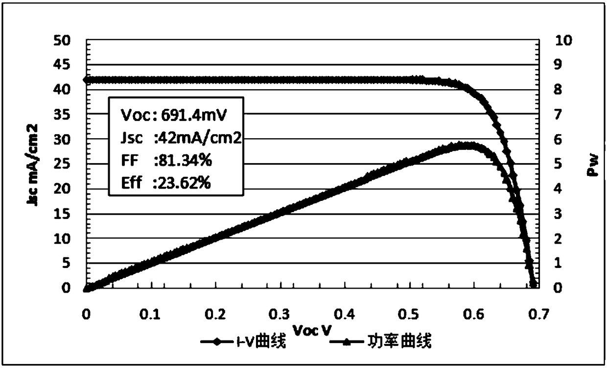
[0044] The present invention will be described in detail below in conjunction with specific embodiments. The following examples will help those skilled in the art to further understand the present invention, but do not limit the present invention in any form. It should be noted that those skilled in the art can make several modifications and improvements without departing from the concept of the present invention. These all belong to the protection scope of the present invention.

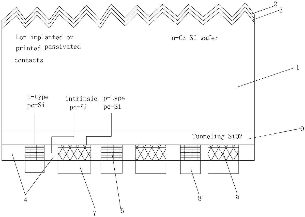
[0045] refer to Figure 1 to Figure 3 , the present invention provides a novel composite structure full back heterojunction solar cell, comprising: N-type silicon substrate 1, silicon nitride film 2, aluminum oxide film 3, intrinsic polysilicon 4, P-type polysilicon 5, N type polysilicon 6, the positive electrode 7 of the battery, the negative electrode 8 of the battery, and the tunneling silicon dioxide passivation layer 9; the front surface of the N-type silicon substrate 1 is covered with an al...


PUM

PropertyMeasurementUnit
Resistivityaaaaaaaaaa
Life expectancyaaaaaaaaaa

Abstract

The invention discloses a novel composite structure full back-side heterojunction solar cell and a preparation method thereof. The solar cell comprises an N-type silicon substrate, a silicon nitride film, an aluminum oxide film, intrinsic polycrystalline silicon, P-type polycrystalline silicon, and N-type polycrystalline silicon. The front surface of the N-type silicon substrate is coated with thealuminum oxide film. The aluminum oxide film is coated with the silicon nitride film. The intrinsic polycrystalline silicon, the P-type polycrystalline silicon, and the N-type polycrystalline siliconare deposited on the back surface of the N-type silicon substrate. The polycrystalline silicon layers are deposited by using horizontally placed silicon wafer LPCVD or horizontally placed silicon wafer PECVD, a homojunction layer can reduce an interface defect state and reduce interface recombination. A laser doping technology is used to realize the P-type polycrystalline silicon layer doping, ensure the service lives of minority carriers of the silicon substrate to the utmost extent and reduce the recombination current density of the contact of metal and silicon. In addition, the cell piecesof the cell with IBC structure fully utilize a solar spectrum to increase the short-circuit current density of the cell to the utmost extent.

Description

technical field [0001] The invention relates to the technical field of manufacturing crystalline silicon solar cells, in particular to a novel composite structure full-back heterojunction solar cell and a preparation method thereof. Background technique [0002] At present, the mainstream technology of mainstream crystalline silicon solar cells is based on polycrystalline black silicon and PERC structure cells. The basic process consists of texturing, diffusion, etching, deposition of anti-reflection film, and screen printing methods on P-type and N-type silicon substrates. Make solar cells. However, the performance of P-type crystalline silicon cells will decline under the influence of oxygen. With the continuous tightening of the global photovoltaic subsidy policy, the market demand for high-performance batteries is becoming more and more strong, while N-type batteries contain less boron, and the performance stability is higher than that of P-type crystalline silicon batt...

Claims


Application Information

Patent Timeline
IPC IPC(8): H01L31/0224H01L31/072
CPCH01L31/022441H01L31/02245H01L31/072Y02E10/50
Inventor 林佳继刘群伊凡·裴力林林依婷
Owner 拉普拉斯新能源科技股份有限公司
Why Eureka
Try Eureka