Method for manufacturing silicon carbide semiconductor device

A semiconductor and silicon carbide technology, which can be used in semiconductor devices, semiconductor/solid-state device manufacturing, electrical components, etc., and can solve problems such as poor characteristics of silicon oxide films.

Inactive Publication Date: 2008-12-31
SUMITOMO ELECTRIC IND LTD
View PDF1 Cites 18 Cited by
  • Summary
  • Abstract
  • Description
  • Claims
  • Application Information

AI Technical Summary

Problems solved by technology

[0003] Meanwhile, a MOSFET including a silicon carbide substrate is disadvantageous in poor characteristics of a silicon oxide film serving as a gate insulating film as compared with a MOSFET (Metal Oxide Semiconductor Field Effect Transistor) including a silicon substrate for the following reason

Method used


Image

  • Method for manufacturing silicon carbide semiconductor device
  • Method for manufacturing silicon carbide semiconductor device
  • Method for manufacturing silicon carbide semiconductor device

Examples


Embodiment approach

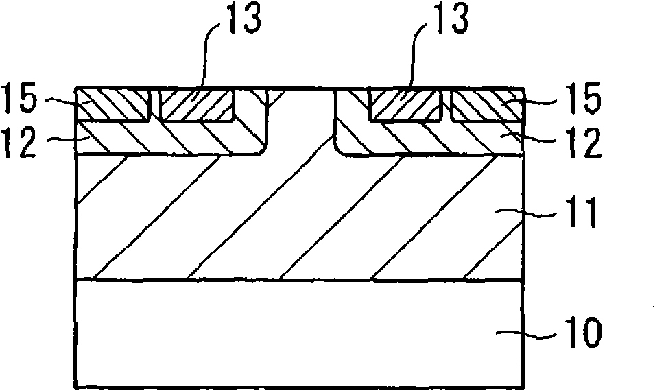
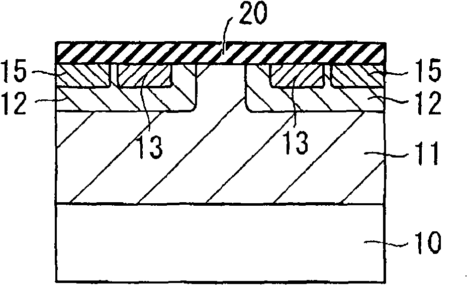
[0029] figure 1 to 6 are cross-sectional views showing steps of manufacturing a MOSFET representing a silicon carbide semiconductor device in the embodiment. although figure 1 to 6 only show two transistor cells representing a part of the vertical MOSFET, but a large number of transistor cells are integrated to constitute one vertical MOSFET.

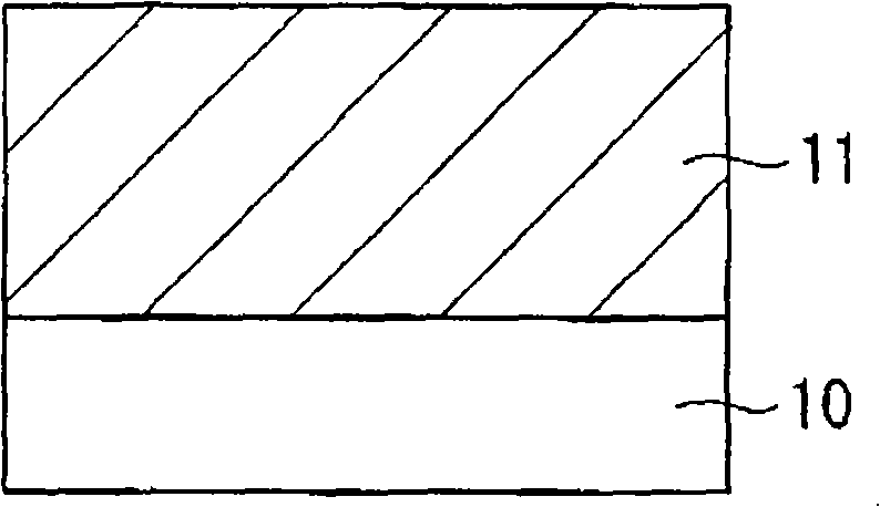
[0030] exist figure 1 In the steps shown, an n-type 4H (hexagonal)-SiC (4 indicates the number of layers stacked in one cycle) substrate 10 is prepared, which has, for example, a resistivity of 0.02 Ωcm and a thickness of 400 μm, and has a thickness in [ The (0001) plane with an inclination angle of about 8° in the 11-20] direction was used as the main surface. Then, using CVD epitaxial growth including in-situ doping, grow on the 4H-SiC substrate 10, for example, containing about 5×10 15 cm -3 concentration of n-type dopant and has an epitaxial growth layer 11 with a thickness of about 10 μm. The outermost surface of the epitaxia...


PUM


Abstract

The invention provides a method for manufacturing a silicon carbide semiconductor device having a small interface state density in the interface region between a gate insulating film (20) and a silicon carbide layer (11). Specifically, an epitaxially grown layer (11) is formed on a 4H-SiC substrate (10), and after that a p well region (12), a source region (13) and a p<+> contact region (15) as ion implanted layers are formed by ion implantation. Then, a gate insulating film (20) composed of a silicon oxide film is formed on the p well region (12), the source region (13) and the p<+> contact region (15) by thermal oxidation or CVD. After that, a plasma is generated by using an N2O-containing gas, which is a gas containing at least one of oxygen and nitrogen, and the gate insulating film (20) is exposed to the plasma.

Description

technical field [0001] The present invention relates to a method of manufacturing a silicon carbide semiconductor device such as a MOSFET having a gate insulating film having a low interface state density. Background technique [0002] Semiconductor devices such as transistors and diodes formed with silicon carbide substrates (SiC substrates) composed of silicon (Si) and carbon (C) bonded to each other at a composition ratio of 1:1 have been expected to be put into use as power devices. in actual use. Since silicon carbide is a wide bandgap semiconductor, its breakdown electric field is an order of magnitude higher than that of silicon. Therefore, even if the depletion layer at the pn junction or Schottky junction has a smaller thickness, a high inversion peak voltage can be maintained. Here, since the use of silicon carbide substrates provides smaller device thicknesses and higher doping concentrations, it is desirable to realize power devices with low on-resistance, high...

Claims


Application Information

Patent Timeline
Patent Type & Authority Applications(China)
IPC IPC(8): H01L21/336H01L21/316H01L29/12H01L29/78
CPCH01J37/3244H01L21/02164H01L21/02236H01L21/02255H01L21/0234H01L21/049H01L29/1608H01L29/518H01L29/66068H01L29/7802H01L21/18H01L21/3065H01L21/3147H01L21/31658H01L21/3148
Inventor 增田健良
Owner SUMITOMO ELECTRIC IND LTD
Why Eureka
Try Eureka