Semiconductor structure and forming method thereof

A technology of semiconductor and gate structure, applied in the field of semiconductor structure and its formation, can solve the problems of difficult channel and poor control ability of gate to channel, so as to improve electrical performance, reduce lattice damage, improve The effect of stress relief

Pending Publication Date: 2020-03-10
SEMICON MFG INT (SHANGHAI) CORP +1
View PDF4 Cites 0 Cited by
  • Summary
  • Abstract
  • Description
  • Claims
  • Application Information

AI Technical Summary

Problems solved by technology

However, as the channel length of the device shortens, the distance between the source and the drain of the device also shortens, so the control ability of the gate to the channel becomes worse, and the difficulty of pinching off the channel by the gate voltage also increases. It is getting bigger and bigger, making subthreshold leakage (subthreshold leakage), the so-called short-channel effect (SCE: short-channel effects) more likely to occur

Method used


Image

  • Semiconductor structure and forming method thereof
  • Semiconductor structure and forming method thereof
  • Semiconductor structure and forming method thereof

Examples


Embodiment Construction

[0030] Semiconductor devices still suffer from poor electrical performance. The reasons for the poor performance of the device are analyzed in conjunction with a method of forming a semiconductor structure.

[0031] refer to Figure 1 to Figure 2 , shows a structural schematic diagram corresponding to each step in a method for forming a semiconductor structure.

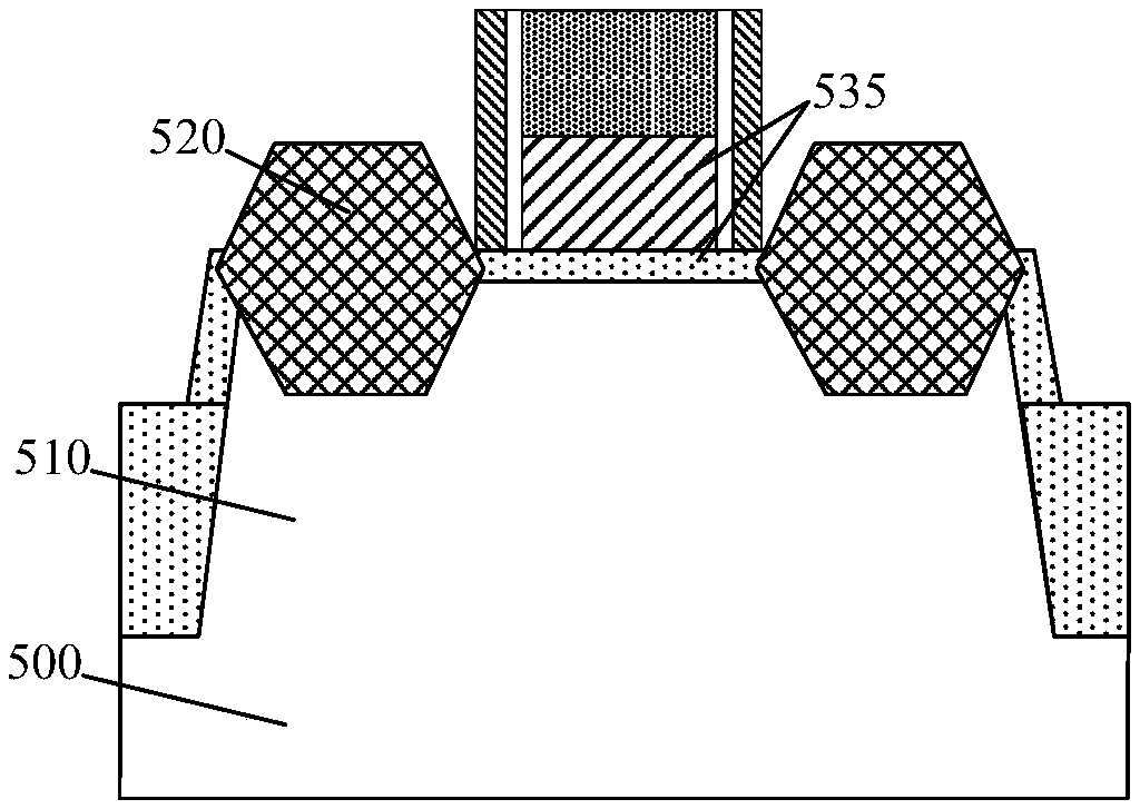
[0032] refer to figure 1 , figure 1 is a cross-sectional view along the extending direction of the fin, providing a base, the base includes a substrate 500, a fin 510 protruding from the substrate 500, a gate structure 535 across the fin 510, and a gate structure 535 located on the The source and drain epitaxial layers 520 in the fins 510 on both sides of the gate structure 535 .

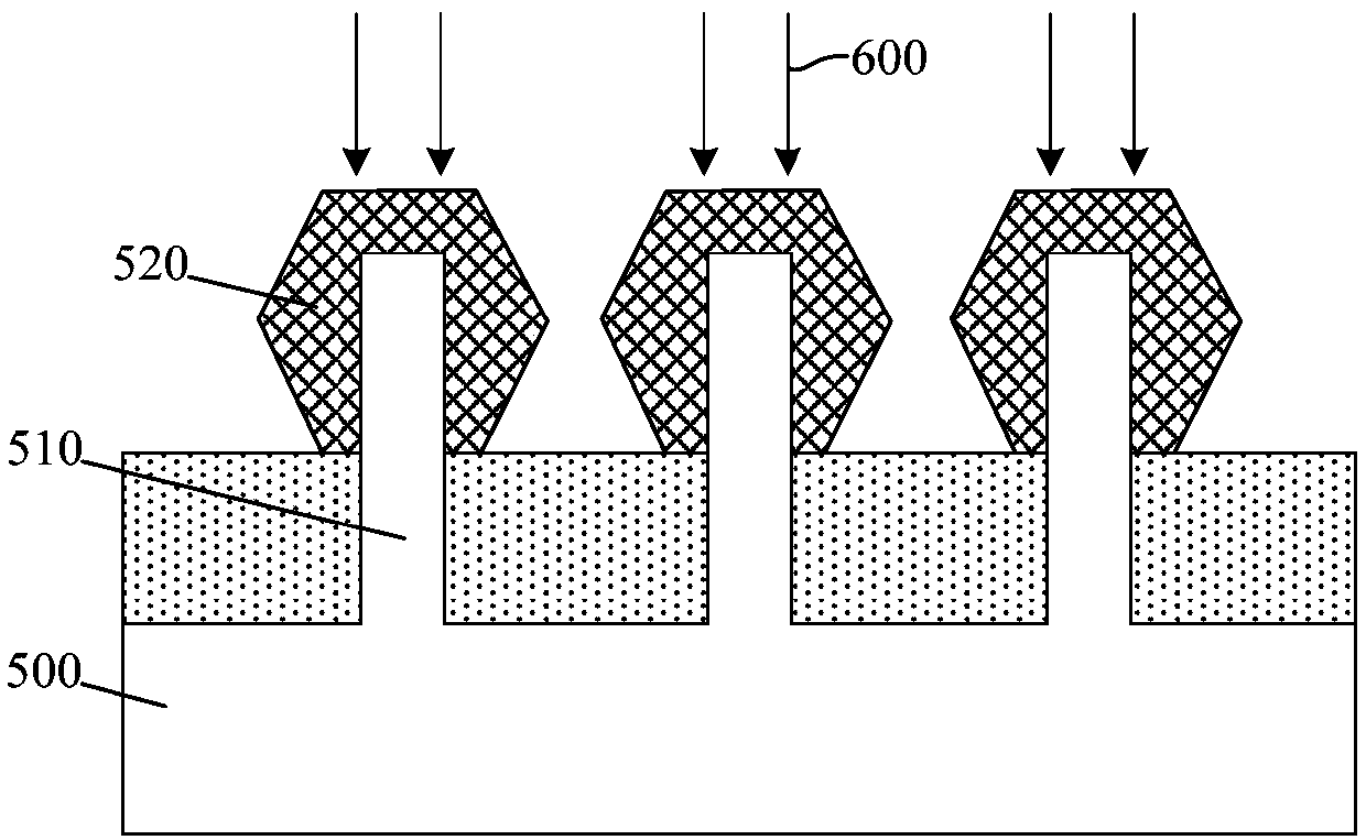
[0033] refer to figure 2 , figure 2 is based on figure 1 Ion doping treatment 600 is performed on the source-drain epitaxial layer 520 along a cross-sectional view perpendicular to the extending direction of the fin.

[0034] Du...


PUM


Abstract

The invention provides a semiconductor structure and a forming method thereof. The forming method comprises the steps: a base is provided, wherein the base comprises a substrate, fin parts protrudingout of the substrate, a gate structure stretching across the fin parts and source and drain epitaxial layers located in the fin parts on the two sides of the gate structure; a protective layer is formed on the substrate exposed out of the gate structure, wherein the protective layer at least covers part of the side wall of the source and drain epitaxial layers and exposes the top of the source anddrain epitaxial layer; and ion doping processing is carried out on the source and drain epitaxial layer exposed out of the protective layer. According to the embodiment of the invention, the protective layer can be used in the step of carrying out ion doping processing on the source and drain epitaxial layer, the side wall of the source and drain epitaxial layer is protected, so that the latticedamage of the source and drain epitaxial layer is reduced, the stress release problem of the source and drain epitaxial layer is correspondingly improved, the carrier mobility is further improved, andthe electrical performance of the semiconductor structure is further improved.

Description

technical field [0001] The invention relates to the field of semiconductor manufacturing, in particular to a semiconductor structure and a forming method thereof. Background technique [0002] With the gradual development of semiconductor process technology, the development trend of semiconductor process nodes following Moore's Law continues to decrease. In order to adapt to the reduction of process nodes, the channel length of MOSFET field effect transistors is also continuously shortened accordingly. However, with the shortening of the channel length of the device, the distance between the source and the drain of the device is also shortened, so the control ability of the gate to the channel becomes worse, and the difficulty of pinching off the channel by the gate voltage also decreases. The larger and larger the subthreshold leakage (subthreshold leakage), the so-called short-channel effect (SCE: short-channel effects) is more likely to occur. [0003] Therefore, in ord...

Claims


Application Information

Patent Timeline
Patent Type & Authority Applications(China)
IPC IPC(8): H01L21/336H01L29/78H01L29/41
CPCH01L29/785H01L29/66795H01L29/41
Inventor 周飞
Owner SEMICON MFG INT (SHANGHAI) CORP
Why Eureka
Try Eureka