4h-sic Metal Semiconductor Field Effect Transistor
A technology of field effect transistors and metal semiconductors, applied in the field of field effect transistors, can solve problems such as saturation current degradation, drain current reduction, lattice damage, etc.
- Summary
- Abstract
- Description
- Claims
- Application Information
AI Technical Summary
Problems solved by technology
Method used
Image

Examples
Embodiment 1
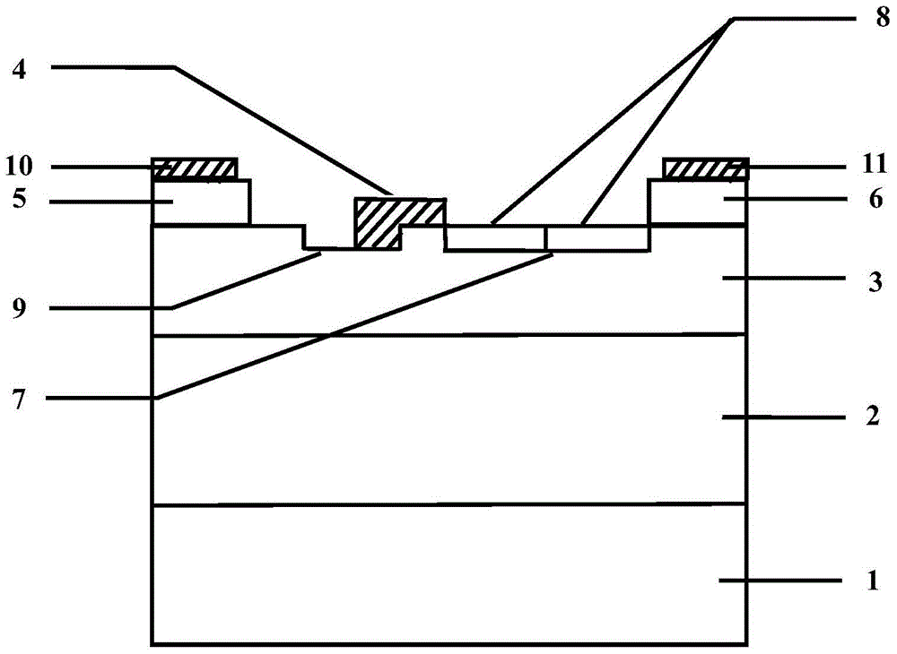
[0036] Example 1: Fabricate a 4H-SiC metal-semiconductor field-effect transistor with a PN junction with a thickness of 0.04 μm and a P region length of 0.45 μm.
[0037] The manufacturing steps of this embodiment are as follows:
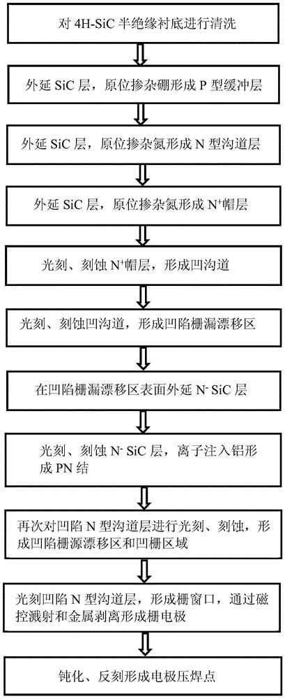
[0038] Step 1: Clean the 4H-SiC semi-insulating substrate to clean the surface.
[0039] (1.1) Carefully clean the substrate twice with a cotton ball dipped in methanol;
[0040] (1.2) Wash the substrate in xylene at 80°C, boiling acetone and methanol at 80°C for 4 minutes, then blow dry with dry high-purity nitrogen;
[0041] (1.3) Place the substrate in H 2 SO 4 with H 2 o 2 After soaking in the mixed solution with a ratio of 1:1 for 10 minutes, rinse twice with deionized water, and finally dry the substrate with nitrogen.
[0042] Step 2: epitaxially grow a SiC layer on the surface of the 4H-SiC semi-insulating substrate, and form a P-type buffer layer by boron in-situ doping.
[0043] Put the 4H‐SiC semi-insulating substrate into the grow...
Embodiment 2
[0076] Example 2: Fabricate a 4H-SiC metal-semiconductor field-effect transistor with a PN junction with a thickness of 0.05 μm and a P region length of 0.5 μm.
[0077] The manufacturing steps of this embodiment are as follows:
[0078] Step 1: Same as Step 1 of Example 1.
[0079] Step 2: Same as Step 2 of Example 1.
[0080] Step 3: Same as Step 3 of Example 1.
[0081] Step 4: Same as Step 4 of Example 1.
[0082] Step 5: Same as Step 5 of Example 1.
[0083] Step 6: Same as Step 6 of Example 1.
[0084] Step 7: Same as Step 7 of Example 1.
[0085] Step 8: Same as Step 8 of Example 1.
[0086] Step 9: Epitaxial N on the surface of the recessed gate drain drift region ‐ SiC layer.
[0087] Simultaneously feed silane at a flow rate of 20ml / min, propane at 10ml / min, high-purity hydrogen at 80l / min and high-purity nitrogen at 2ml / min in the growth chamber at a growth temperature of 1550°C and a pressure of 10 5 Under the condition of Pa for 36s, grow 0.05μm thick N ...
Embodiment 3
[0094] Example 3: Fabricate a 4H-SiC metal-semiconductor field-effect transistor with a PN junction with a thickness of 0.045 μm and a P region length of 0.48 μm.
[0095] The manufacturing steps of this embodiment are as follows:
[0096] Step A: Same as Step 1 of Example 1.
[0097] Step B: Same as Step 2 of Example 1.
[0098] Step C: Same as Step 3 of Example 1.
[0099] Step D: Same as Step 4 of Example 1.
[0100] Step E: Same as Step 5 of Example 1.
[0101] Step F: Same as Step 6 of Example 1.
[0102] Step G: Same as Step 7 of Example 1.
[0103] Step H: Same as Step 8 of Example 1.
[0104] Step I: Epitaxial N on the surface of the recessed gate drain drift region ‐ SiC layer.
[0105] Simultaneously feed silane at a flow rate of 20ml / min, propane at 10ml / min, high-purity hydrogen at 80l / min and high-purity nitrogen at 2ml / min in the growth chamber at a growth temperature of 1550°C and a pressure of 10 5 Under the condition of Pa for 33s, the growth of 0.045...
PUM
 Abstract
Description
Claims
Application Information