Method of forming oxide film

a technology of oxide film and wet oxidation method, which is applied in the manufacturing of basic electric elements, semiconductor/solid-state devices, electric devices, etc., can solve the problems of reducing the electric characteristics and reliability of semiconductor devices, the thickness of silicon oxide film is not uniform, and the content of residual cleaning solution is not uniform, so as to prevent the surface roughening of semiconductor layers

Inactive Publication Date: 2001-10-02
SONY CORP
View PDF7 Cites 126 Cited by
  • Summary
  • Abstract
  • Description
  • Claims
  • Application Information

AI Technical Summary

Benefits of technology

It is therefore an object of the present invention to provide a method of forming an oxide film, which method enables the formation of a so-called wet oxide film as a protective oxide film for preventing the surface roughening of a semiconductor layer.
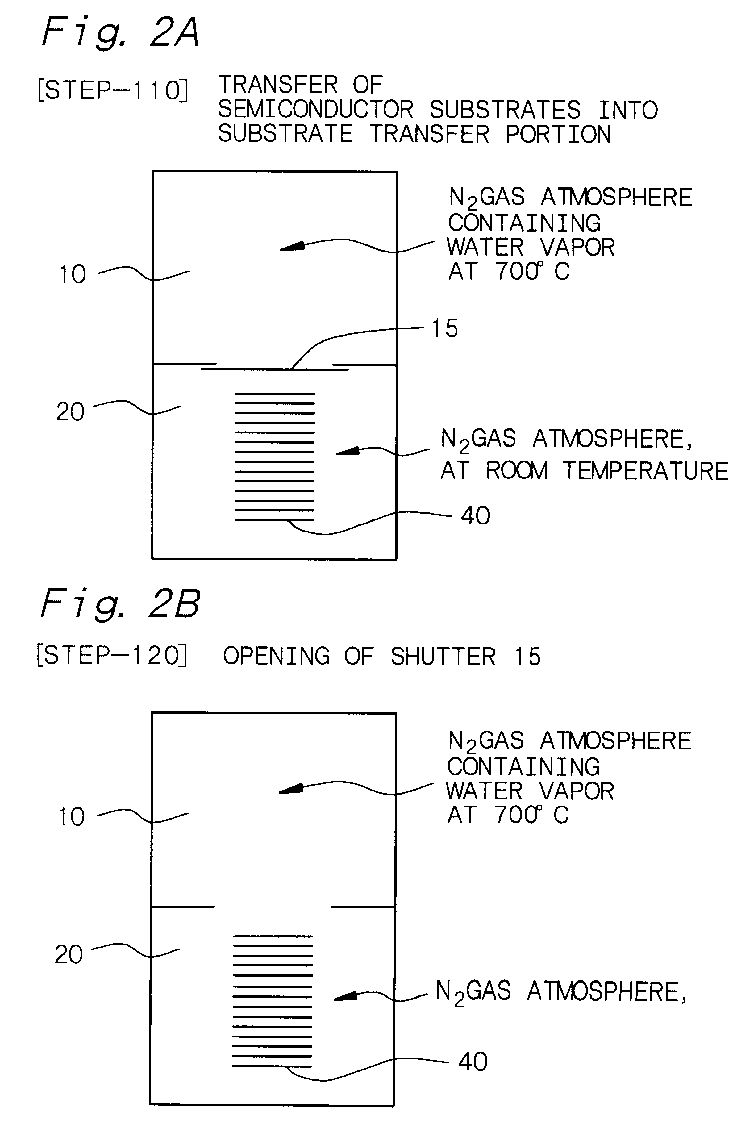
As already described, it is required to prevent the surface roughening (concavo-convex surface) of a silicon semiconductor substrate. In the present invention, the process chamber in the step (B) has a water vapor atmosphere when the substrate is transferred into the process chamber. Therefore, the formation of a so-called dry oxide film on the semiconductor layer can be reliably prevented, and an oxide film having excellent properties can be formed.
When the temperature of the process-chamber atmosphere in the step (C) is set approximately at the same level as that in the step (A), and when an oxide film is formed on the semiconductor layer on the surface of the substrate during the transfer of the substrate into the process chamber, the thus-formed oxide film works as a protective oxide film to prevent the surface roughening of the semiconductor layer when the temperature of the semiconductor layer is increased. When the temperature of the process-chamber atmosphere in the step (C) is to be set at a level higher than that in the step (A), it is required to increase the temperature of the process-chamber atmosphere after completion of the step (B). An oxide film is pre-formed on the semiconductor layer on the surface of the substrate during the transfer of the substrate into the process chamber in the step (B), or an oxide film is pre-formed at any time from the initiation of the step (B) to the initiation of an increase in temperature. In this case, the thus-formed oxide film works as a protective oxide film to prevent the surface roughening of the semiconductor layer when the temperature is increased. The oxide film thus-formed on the semiconductor layer on the surface of the substrate during the transfer of the substrate into the process chamber in the step (B), or the oxide film thus-formed at any time from the initiation of the step (B) to the initiation of an increase in temperature will be referred to as "initial oxide film" for the convenience.
Generally, before the formation of the oxide layer on a surface of a silicon semiconductor substrate, the surface of the silicon semiconductor substrate is cleaned by RCA cleaning in which it is cleaned with an NH.sub.4 OH / H.sub.2 O.sub.2 aqueous solution and further cleaned with an HCl / H.sub.2 O.sub.2 aqueous solution, to remove fine particles and metal impurities from its surface, and then the surface of the silicon semiconductor substrate is cleaned with a hydrofluoric acid aqueous solution and pure water. When the silicon semiconductor substrate is exposed to atmosphere thereafter, the surface of the silicon semiconductor substrate may be contaminated, or water or an organic substance may adhere to the surface of the silicon semiconductor substrate, or Si atoms in the surface of the silicon semiconductor substrate may be bonded to hydroxyl groups (OH) (for example, see the literature of "Highly-reliable Gate Oxide Formation for Giga-Scale LSIs by using Closed Wet Cleaning System and Wet Oxidation with Ultra-Dry Unloading", J. Yugami, et al., International Electron Device Meeting Technical Digest 95, pp 855-858). In such a case, when the formation of an oxide film is initiated in such a state, the formed oxide film contains water or an organic substance or contains, for example, Si--OH, which can cause the formed oxide film to degrade in properties or to have a defective portion. The defective portion refers to an oxide film portion containing a defect such as a silicon dangling bond (Si.) or an Si--H bond, or an oxide film portion containing Si--O--Si bonds which are compressed due to a stress or Si--O--Si bonds having a bond angle different from the angle of Si--O--Si bonds of a thick or bulky silicon oxide film. For avoiding the above problems, preferably, the method of the present invention includes the step of cleaning the surface of the semiconductor layer before the formation of the oxide film, and the formation of the oxide film is carried out without exposing the cleaned semiconductor layer to atmosphere (i.e., for example, using an inert gas atmosphere or a vacuum atmosphere as an atmosphere from the cleaning of the surface of the semiconductor layer to the initiation of the step of forming the oxide film). In this manner, for example, when a silicon semiconductor substrate is used as a semiconductor layer, an oxide film can be formed on a surface of a silicon semiconductor substrate most of which is terminated with hydrogen and a very small part of which is terminated with fluorine, and degradation of the formed oxide film in characteristics or occurrence of the defective portion can be prevented.

Problems solved by technology

When the amount ratio of the natural oxide film contained in the oxide film increases with a decrease in the oxide film, the oxide film formed by the wet oxidation method deteriorates in electric characteristics.
Since, however, the natural oxide film works as a protective oxide film on one hand, it may cause a decrease in the electric characteristics and reliability of a semiconductor device if the formation of the natural oxide film is simply suppressed.
The thus-formed silicon oxide film has a non-uniform thickness and has a residual cleaning solution content.
Meanwhile, when a silicon semiconductor substrate is exposed to a high-temperature inert gas or vacuum atmosphere, the silicon semiconductor substrate is caused to have a roughened surface due to the elimination of silicon atoms and fluorine atoms from the silicon semiconductor substrate and a nitriding reaction in the silicon semiconductor substrate, so that the oxide film is poor in an electric insulation property and reliability.

Method used


Image

  • Method of forming oxide film
  • Method of forming oxide film
  • Method of forming oxide film

Examples


example 2

FIG. 5 shows a conceptual view of a horizontal type oxide film forming apparatus for forming an oxide film according to a pyrogenic oxidation method. The oxide film forming apparatus has a process chamber 50 and a resistance heater which is heating means 51 for heating a semiconductor layer. The process chamber 50 is made of a quartz furnace core tube and is for receiving a semiconductor layer (specifically, a silicon semiconductor substrate 40) therein for forming an oxide film on the semiconductor layer. The resistance heater as heating means 51 is disposed outside the process chamber 50 and is disposed nearly in parallel with the surface of the semiconductor layer. The semiconductor layer (for example, a silicon semiconductor substrate 40) is placed on a wafer stage 52. It is transferred into and out of the process chamber 50 through a gate valve 53 which is the partitioning means disposed on one end of the process chamber 50. The oxide film forming apparatus has a gas inlet port...


PUM


Abstract

A method of forming an oxide film comprising the steps of; (A) generating a water vapor atmosphere in a process chamber in a state where partitioning means is closed, and transferring a substrate into a substrate transfer portion, (B) opening the partitioning means after the transfer of the substrate into the substrate transfer portion is completed, and transferring the substrate into the process chamber having the water vapor atmosphere, (C) thermally oxidizing a semiconductor layer on the surface of the substrate in the process chamber having the water vapor atmosphere, to form an oxide film having a predetermined thickness on the surface of the semiconductor layer, and (D) changing the atmosphere in the process chamber into an inert gas atmosphere, then transferring the substrate out of the process chamber, closing the partitioning means and transferring the substrate out of the substrate transfer portion.

Description

BACKGROUND OF THE INVENTION AND RELATED ART STATEMENTThe present invention relates to a method of forming an oxide film on a semiconductor layer on a surface of a substrate in the production of a semiconductor device.For example, in producing a MOS type silicon semiconductor device on the basis of a silicon semiconductor substrate, it is required to form a gate oxide film composed of a silicon oxide film (SiO.sub.2 film) on a surface of the silicon semiconductor substrate. In the production of a thin film transistor (TFT), it is also required to form a gate oxide film composed of a silicon oxide film (SiO.sub.2 film) on a surface of a silicon layer formed on an insulating substrate. It is no exaggeration to say that the reliability of semiconductor devices depends upon these silicon oxide films. The silicon oxide films are therefore constantly required to have high dielectric breakdown durability and long-term reliability. In a MOS type silicon semiconductor device, a silicon oxide ...

Claims


Application Information

Patent Timeline
Patent Type & Authority Patents(United States)
IPC IPC(8): H01L21/02H01L21/316H01L21/31
CPCH01L21/02238H01L21/02255H01L21/02307H01L21/31662
Inventor KASHIWAGI, AKIHIDE
Owner SONY CORP
Why Eureka
Try Eureka