Manufacturing method of GaN field effect transistor

A gallium nitride field and manufacturing method technology, which is applied in semiconductor/solid-state device manufacturing, semiconductor devices, electrical components, etc., can solve problems such as rough surface and poor edge morphology, and achieve good uniformity and reliability of withstand voltage high effect

Inactive Publication Date: 2017-10-03
PEKING UNIV +2
View PDF2 Cites 2 Cited by
  • Summary
  • Abstract
  • Description
  • Claims
  • Application Information

AI Technical Summary

Problems solved by technology

[0004] The invention provides a method for manufacturing GaN field-effect transistors to solve the problems in the prior art that some metal layers in ohmic electrodes have rough surfaces and poor edge morphology caused by high-temperature annealing process

Method used


Image

  • Manufacturing method of GaN field effect transistor
  • Manufacturing method of GaN field effect transistor
  • Manufacturing method of GaN field effect transistor

Examples


Embodiment 1

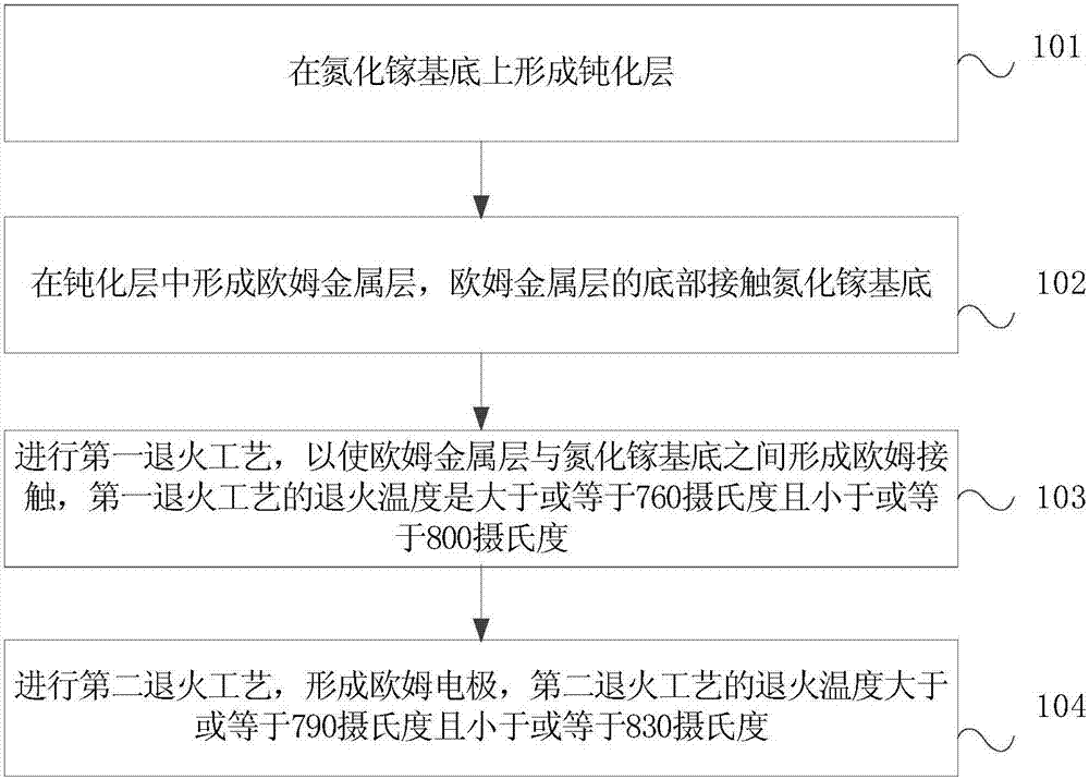
[0033] This embodiment provides a method for manufacturing a GaN field effect transistor, which is used for manufacturing a GaN field effect transistor.

[0034] Such as figure 1 As shown, is a schematic flow chart of the fabrication method of the eGaN field effect transistor according to the present embodiment. The fabrication method of the gallium nitride field effect transistor of this embodiment includes:

[0035] Step 101, forming a passivation layer on a GaN substrate.

[0036] The gallium nitride substrate may be any substrate used for manufacturing gallium nitride field effect transistors in the prior art. In this embodiment, the gallium nitride substrate includes a Si substrate, a GaN layer and an AlGaN layer formed sequentially from bottom to top.

[0037] The passivation layer in this embodiment is used to protect the metal surface from being oxidized, thereby delaying the corrosion rate of the metal and improving the reliability of the semiconductor device. The...

Embodiment 2

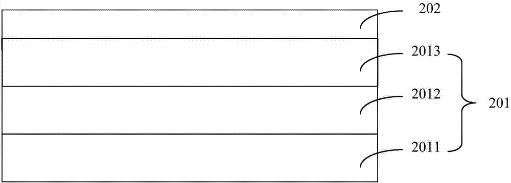
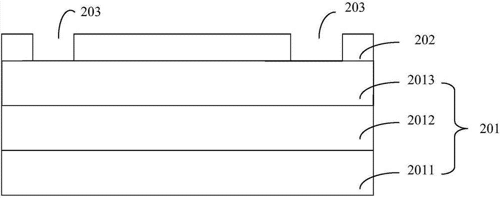
[0046] In this embodiment, a further supplementary explanation is given to the fabrication method of the eGaN field effect transistor in the above embodiments. Such as Figures 2A to 2G Shown is a structural schematic diagram of each step in the manufacturing method of the eGaN field effect transistor according to the present embodiment.

[0047] Such as Figure 2A As shown, a passivation layer 202 is formed on a GaN substrate 201 .

[0048] In this embodiment, the gallium nitride substrate 201 includes a Si substrate 2011 , a GaN layer 2012 and an AlGaN layer 2013 which are sequentially formed from bottom to top. Specifically, a layer of Si may be formed on the surface of the barrier layer of the AlGaN layer 2013. 3 N 4 layer as a passivation layer 202.

[0049] Such as Figure 2BAs shown, an ohmic contact hole 203 is formed in the passivation layer 202 to expose the gallium nitride substrate 201, and the ohmic contact hole 203 is surface treated.

[0050] For example,...


PUM


Abstract

The invention provides a manufacturing method of a GaN field effect transistor. The method comprises the following steps: forming a passivation layer on a GaN substrate; forming an ohmic metal layer in the passivation layer, wherein the bottom of the ohmic metal layer is contacted with the GaN substrate; performing the first annealing process so as to form the ohmic contact between the ohmic metal layer and the GaN substrate, wherein the annealing temperature of the first annealing process is greater than or equal to 760 DEG C and less than and equal to 800 DEG C; performing the second annealing process to form an ohmic electrode, wherein the annealing temperature of the second annealing process is greater than or equal to the 790 DEG C and less than or equal to 830 DEG C. By using the manufacturing method of the GaN field effect transistor provided by the embodiment, the good ohmic contact and good edge morphology can be formed, the voltage withstand uniformity of the GaN field effect transistor is good, and the reliability is high.

Description

technical field [0001] The invention relates to semiconductor technology, in particular to a method for manufacturing a gallium nitride field effect transistor. Background technique [0002] Power devices featuring low power consumption and high speed have recently attracted a lot of attention as the need for efficient and complete power conversion circuits and systems has increased. GaN is the third generation wide bandgap semiconductor material, because of its large bandgap width (3.4eV), high electron saturation rate (2e 7 cm / s), high breakdown electric field (1e 10 -3e 10 V / cm), high thermal conductivity, corrosion resistance and radiation resistance, etc., have strong advantages in high pressure, high frequency, high temperature, high power and radiation resistance environmental conditions, and are considered to be researched on short-wave optoelectronic devices and high voltage The best material for high frequency high power devices. Therefore, the Gallium Nitride ...

Claims


Application Information

Patent Timeline
Patent Type & Authority Applications(China)
IPC IPC(8): H01L29/45H01L21/335H01L21/285
CPCH01L29/452H01L21/28575H01L29/66446
Inventor 刘美华孙辉林信南陈建国
Owner PEKING UNIV
Why Eureka
Try Eureka