High voltage isolated n-type ldmos device and method of manufacturing the same

A high-voltage isolation, N-type technology, used in semiconductor/solid-state device manufacturing, semiconductor devices, electrical components, etc., can solve the problem of high cost, achieve the effect of performance improvement, simple and flexible process, and cost reduction

Active Publication Date: 2016-06-08
SHANGHAI HUAHONG GRACE SEMICON MFG CORP
View PDF5 Cites 0 Cited by
  • Summary
  • Abstract
  • Description
  • Claims
  • Application Information

AI Technical Summary

Problems solved by technology

[0012] In view of this situation, most of the prior art adopts the process method of N-type buried layer + epitaxy to meet the punch-through requirements of the PNP (Pbody-DNW-P-type substrate) of the device in the vertical direction; (draindrift), using the Resurf method to design, in order to achieve the optimization of the withstand voltage and specific on-resistance (Rdson) of the device, so as to improve the performance of the device, but, using the N-type buried layer + epitaxy process method, and Resurf's method, more expensive

Method used


Image

  • High voltage isolated n-type ldmos device and method of manufacturing the same
  • High voltage isolated n-type ldmos device and method of manufacturing the same

Examples


Embodiment Construction

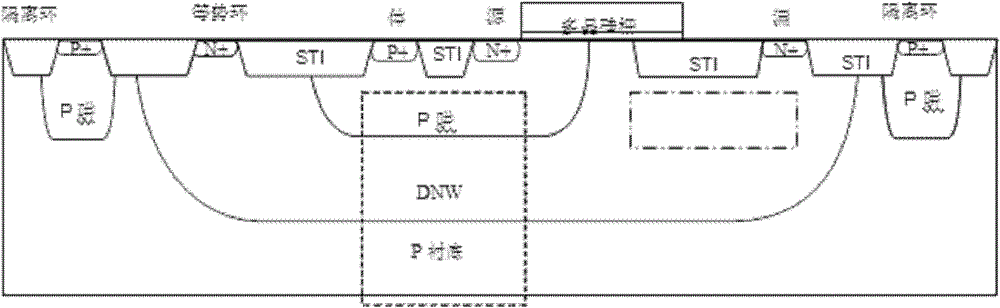
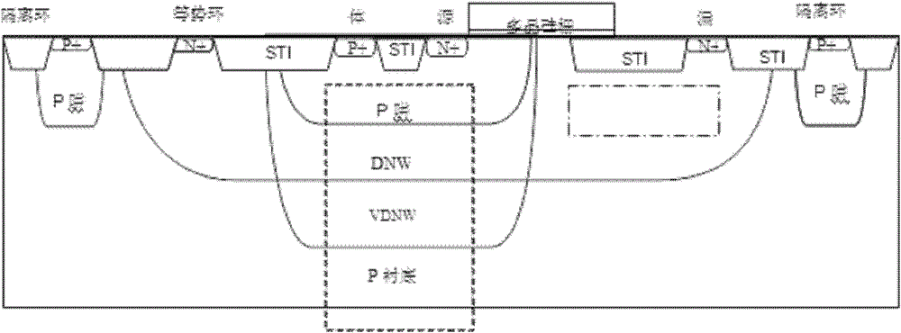
[0028] An embodiment of the high-voltage isolation N-type LDMOS device of the present invention is figure 2 As shown, a deep N-type well DNW is formed on the P-type substrate, and a very deep N-type well VDNW deeper than the deep N-type well DNW is formed in the deep N-type well DNW. A P-type well is formed in the N-type well VDNW, a polysilicon gate is formed above the adjacent region of the P-type well and the deep N-type well DNW, and a polysilicon gate is formed on the P-type well located on one side of the polysilicon gate. The source terminal and the body terminal are formed with a drain terminal on the deep N-type well on the opposite side of the polysilicon gate. figure 2 In the dotted line area is the PNP (Pbody-DNW-P type substrate) structure in the vertical direction, and the dotted line area is the drain terminal N-type drift region (draindrift).

[0029] Preferably, the depth of the deep N-type well is one-third to three-quarters of the depth of the very deep N...


PUM


Abstract

The invention discloses a high-voltage isolating N-type LDMOS (Laterally Diffused Metal Oxide Semiconductor) device. A deep N well is formed on a P substrate; a very deep N well deeper than the deep N well is formed in the deep N well; a P body is formed in the very deep N well; a polysilicon gate is formed above an adjacent region between the P body and the deep N well; a device source and a device body are formed on the P body located on one side of the polysilicon gate; and a device drain is formed on the deep N well located on the opposite side of the polysilicon gate. The invention further discloses a manufacturing method of the high-voltage isolating N-type LDMOS device. The withstand voltage of the high-voltage isolating N-type LDMOS device can be ensured under a small lateral dimension, the specific on resistance is optimized, and the cost is low.

Description

technical field [0001] The invention relates to semiconductor technology, in particular to a high-voltage isolation N-type LDMOS device and a manufacturing method thereof. Background technique [0002] High-voltage isolation N-type LDMOS (Lateral Double-diffused Metal-Oxide Semiconductor) devices are widely used in power management chip design due to their advantages of flexible design, low specific on-resistance (Rdson), and fast response speed. Compared with ordinary N-type LDMOS devices, high-voltage isolation N-type LDMOS devices will perform deep N-type well (DeepNwell, DNW) implantation under the P-type well (Pbody) region for isolation purposes. Therefore, the potential connected to the source (source, N+) of the high-voltage isolated N-type LDMOS and the P-type well lead-out (bulk) can be connected at the potential (generally Vdd) of the zero potential (ground) and the drain (drain). , floating between the highest potential of the line). However, the source termina...

Claims


Application Information

Patent Timeline
Patent Type & Authority Patents(China)
IPC IPC(8): H01L29/06H01L29/78H01L21/336
Inventor 刘剑段文婷孙尧陈瑜陈华伦
Owner SHANGHAI HUAHONG GRACE SEMICON MFG CORP
Why Eureka
Try Eureka