High voltage p-type ldmos structure and fabrication method thereof
A manufacturing method and high-voltage technology, applied in semiconductor/solid-state device manufacturing, electrical components, circuits, etc., can solve the problems of unfavorable chip designers, increased costs, and sacrificed area, and achieve the effect of reducing the need for PNP punch-through and reducing the area
- Summary
- Abstract
- Description
- Claims
- Application Information
AI Technical Summary
Problems solved by technology
Method used
Image
Examples
Embodiment Construction
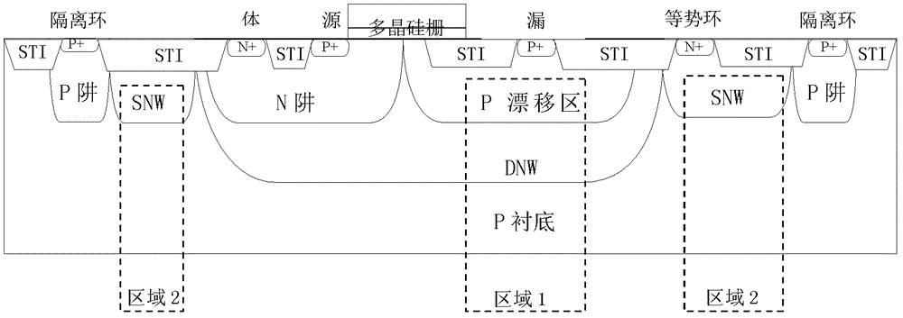
[0028] The cross-sectional view of an embodiment of the high-voltage P-type LDMOS structure of the present invention is as follows figure 2 As shown, area 1 is a PNP (P drift-DNW-P type substrate) structure in the vertical direction, and area 2 is an effective isolation area from the equipotential ring (guard ring) to the isolation ring (Isolation ring). A deep N well (Deep N well, DNW) is formed on the P-type silicon substrate, and an N well is formed in the left part of the deep N well, and a source terminal and a body terminal are formed on the N well. A P drift region is formed in the right part of the deep N well, and a drain terminal is formed on the P drift region. The left and right shallow N wells (shallow N well, SNW) are respectively formed adjacent to the left and right sides of the deep N well. and the right shallow N well, a P-type isolation ring (isolation ring) is formed on the left side of the left shallow N well and the right side of the right shallow N well...
PUM
 Abstract
Description
Claims
Application Information

