Supercharge Your Innovation With Domain-Expert AI Agents!

Touch sensing structure and manufacturing method thereof

A technology of touch sensing and manufacturing method, which is applied to instruments, electrical digital data processing, input/output process of data processing, etc., and can solve the problems of open circuit, difficulty in improving the signal transmission sensitivity of touch sensing structure, and energy consumption.

Inactive Publication Date: 2016-05-04
RTR TECH TECH
View PDF8 Cites 0 Cited by
  • Summary
  • Abstract
  • Description
  • Claims
  • Application Information

AI Technical Summary

Problems solved by technology

When the ITO impedance is large, it will be difficult to improve the signal transmission sensitivity of the touch sensing structure
The ITO area resistance of most flexible conductive substrates is above 150 ohms / square. Since the substrates used in flexible conductive substrates are mostly made of plastic materials, such as PET, their heat resistance temperature cannot be compared with that of glass substrates. However, high-temperature annealing cannot be used to crystallize ITO, so that the surface resistance of the soft conductive substrate cannot be reduced.
However, although the ITO on the glass substrate can be crystallized by high-temperature annealing process to reduce the surface resistance of ITO, the production process is also quite time-consuming and energy-consuming.
[0004] The sensing electrode of another known capacitive touch panel is a metal mesh sensing structure composed of a plurality of metal wires. Compared with ITO, the metal mesh sensing structure has lower impedance; however, in this case In the design, it is easy to interrupt the electrical connection of the sensing structure due to the disconnection of the metal wire in the manufacturing process, resulting in an open circuit

Method used


Image

  • Touch sensing structure and manufacturing method thereof
  • Touch sensing structure and manufacturing method thereof
  • Touch sensing structure and manufacturing method thereof

Examples


Embodiment Construction

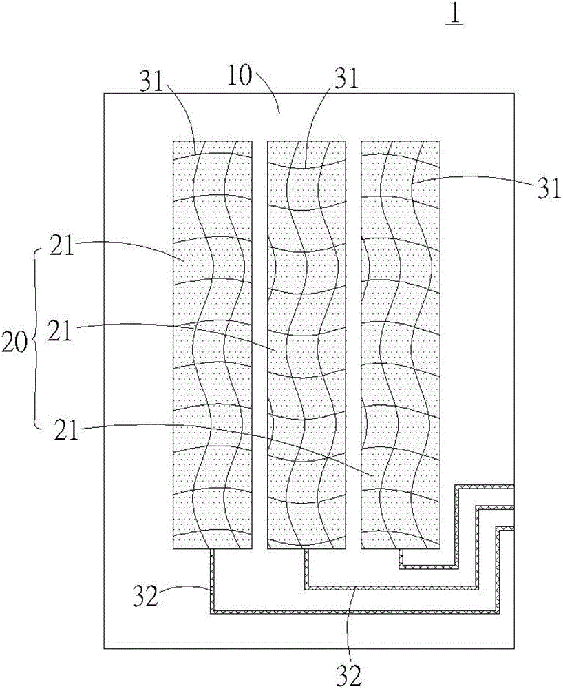
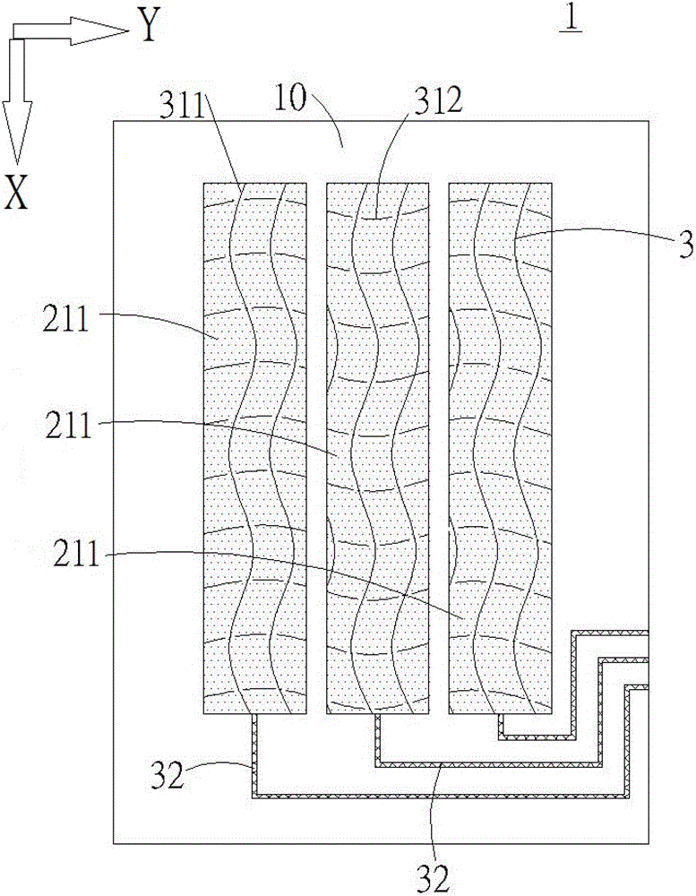
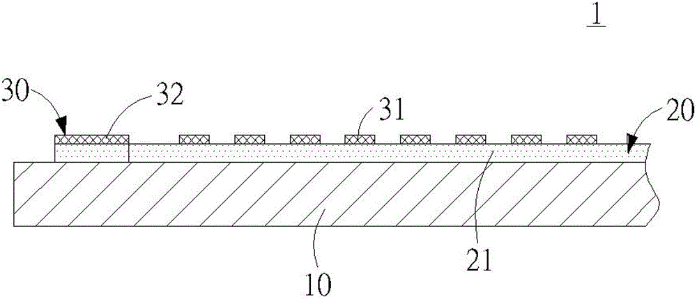
[0041] like figure 1 Structural schematic diagram of the touch sensing structure in the touch panel of the present invention, figure 2 As shown in the cross-sectional view of the touch sensing structure in the touch panel of the present invention, in an embodiment of the present invention, the touch sensing structure 1 includes: a transparent substrate 10, a transparent conductive layer 20 and a conductive auxiliary structure 31, wherein the transparent substrate 10 is made of a rollable material, which can be rolled into a roll shape. The material of the transparent substrate 10 can be, for example, one of PEN, PET, PES, windable glass, PMMA, PC or PI, or it can be a multi-layer composite material of the above-mentioned materials, and multiple layers can also be formed on the above-mentioned materials. The substrate of the transparent stack structure, the multi-layer transparent stack structure may be an anti-reflection layer or an anti-glare layer, for example. Alternativ...


PUM


Abstract

The invention provides a touch sensing structure which comprises a transparent substrate; a transparent conducting layer which is disposed on the transparent substrate and is provided with a plurality of sensing structures; conducting auxiliary structures which are disposed on the plurality of sensing structures and are used for increasing the conductivity of the plurality of sensing structures; a plurality of filling structures which are located between the plurality of sensing structures and below the conducting auxiliary structures, and are open electrically with the plurality of sensing structures; and a plurality of peripheral circuits which are electrically connected with the sensing structures respectively, and are used for connecting soft circuit boards.

Description

technical field [0001] The invention provides a touch sensing structure and a manufacturing method thereof, which can improve the optical performance and sensitivity of a touch panel, and can greatly improve the production yield of the touch sensing structure. Background technique [0002] Press, the current touch input methods of the touch panel (TouchPanel) in the market include resistive, capacitive, optical, electromagnetic induction, sound wave induction, etc.; Touch the surface of the panel with a finger or a sensor pen, and a capacitance value change is generated inside the panel at the touched position, so as to detect the touched position on the surface of the panel to achieve the purpose of touch sensing. [0003] It is known that, in order to detect the position where the user touches the touch panel with a finger or a stylus, various capacitive touch sensing structures have been developed by the industry. The sensing electrodes of the conventional capacitive tou...

Claims


Application Information

Patent Timeline
Patent Type & Authority Patents(China)
IPC IPC(8): G06F3/041G06F3/044
Inventor 陈维钏郭晓文
Owner RTR TECH TECH
Features
  • R&D
  • Intellectual Property
  • Life Sciences
  • Materials
  • Tech Scout
  • Unparalleled Data Quality
  • Higher Quality Content
  • 60% Fewer Hallucinations
Learn More