An Insulated Gate Bipolar Transistor

A technology of bipolar transistors and insulated gates, applied in semiconductor devices, electrical components, circuits, etc., can solve the problems that holes cannot be drawn away, device temperature rises, and devices burn out, etc.

Active Publication Date: 2016-03-30
HUAWEI TECH CO LTD
View PDF3 Cites 0 Cited by
  • Summary
  • Abstract
  • Description
  • Claims
  • Application Information

AI Technical Summary

Problems solved by technology

For the situation of widely used inductive loads, since the inductor current cannot be mutated, that is, the current flowing through the IGBT cannot be mutated, so all the current flowing through the IGBT must be provided by the hole current formed by the holes injected into the drift region by the collector. , for the terminal region of the IGBT device, a large number of holes are injected into the drift region from the collector of the device. However, the injected holes cannot be directly drawn away from the floating field ring structure of the terminal, but at the equipotential ring of the terminal concentration, resulting in longer hole recombination time, slower turn-off speed, and increased turn-off loss; in addition, a local accumulation effect of hole current is formed at the equipotential ring of the terminal, resulting in local high voltage and large current, causing the device temperature to sharply increase Rising, causing dynamic avalanche breakdown and thermal breakdown of the device, causing the device to burn

Method used


Image

  • An Insulated Gate Bipolar Transistor
  • An Insulated Gate Bipolar Transistor
  • An Insulated Gate Bipolar Transistor

Examples


Embodiment 1

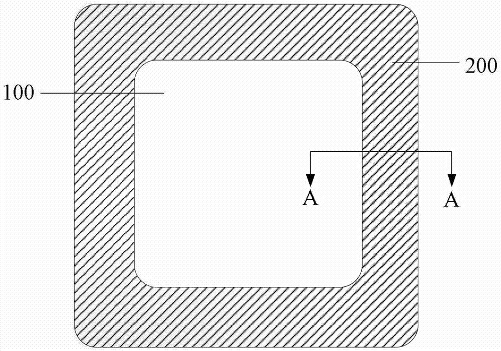
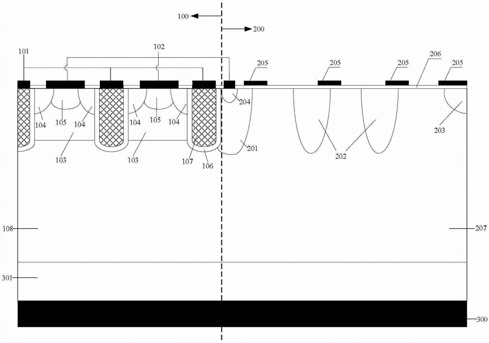
[0042] Embodiment one, such as image 3 As shown, an IGBT provided by Embodiment 1 of the present invention includes: a cell region 100 and a terminal region 200 surrounding the cell region. The cell region 100 includes a gate 101, an emitter 102, a p well region 103, an n+ emitter region 104 and a p+ emitter region 105 contained in the p well region 103 in contact with the emitter, a trench gate Region 107, gate oxide region 106, and oxide isolation layer region 206; wherein, a plurality of trench-type gate regions 107 are connected together by metal to form the gate 101 of IGBT; p well region 103 and contained in p well region The n+ emitter region 104 and the p+ emitter region 105 in 103 are connected together by metal to form the emitter 102 of the IGBT. The terminal region 200 includes a first field ring p region 201, several field ring p regions 202, a p+ region 204 connected to the emitter 102, a field plate region 205, an equipotential ring n region 203 located at the...

Embodiment 2

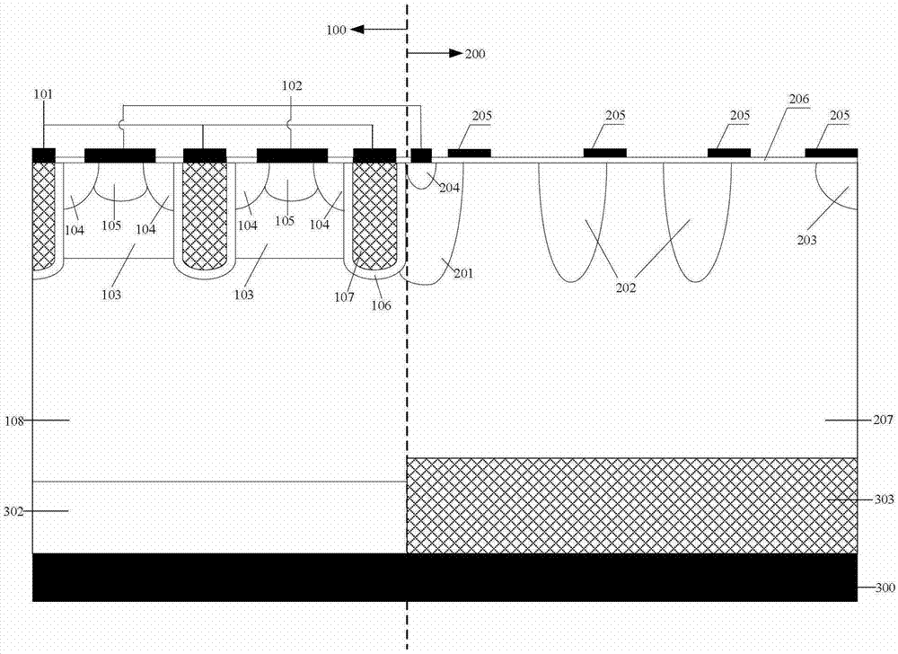
[0060] Embodiment two, such as Figure 5As shown, an IGBT provided by Embodiment 2 of the present invention includes: a cell region 100 and a terminal region 200 surrounding the cell region. The cell region 100 includes a gate 101, an emitter 102, a p well region 103, an n+ emitter region 104 and a p+ emitter region 105 contained in the p well region 103 in contact with the emitter, a trench gate Region 107, gate oxide region 106, and oxide isolation layer 206; wherein, a plurality of trench gate regions 107 are connected together by metal to form the gate 101 of the IGBT; p well region 103 and contained in p well region 103 The inner n+ emitter region 104 and p+ emitter region 105 are connected together by metal to form the emitter 102 of the IGBT. The terminal region 200 includes a first field ring p region 201, several field ring p regions 202, a p+ region 204 connected to the emitter 102, a field plate region 205, an equipotential ring n region 203 located at the edge of ...

Embodiment 3

[0075] Embodiment three, such as Figure 10 As shown, an IGBT provided by Embodiment 3 of the present invention includes: a cell region 100 and a terminal region 200 surrounding the cell region. The cell region 100 includes a gate 101, an emitter 102, a p well region 103, an n+ emitter region 104 and a p+ emitter region 105 contained in the p well region 103 in contact with the emitter, a trench gate Region 107, gate oxide region 106, and oxide isolation layer 206; wherein, a plurality of trench gate regions 107 are connected together by metal to form the gate 101 of the IGBT; p well region 103 and contained in p well region 103 The inner n+ emitter region 104 and p+ emitter region 105 are connected together by metal to form the emitter 102 of the IGBT. The terminal region 200 includes a first field ring p region 201, several field ring p regions 202, a p+ region 204 connected to the emitter 102, a field plate region 205, an equipotential ring n region 203 located at the edge...


PUM


Abstract

Embodiments of the present invention provide an IGBT, which relates to the field of integrated circuit manufacturing, and may improve a problem of tail current when the IGBT is turned off. The IGBT includes a cell region on a front surface, a terminal region surrounding the cell region, an IGBT drift region of a first conductivity type, and an IGBT collector region on a back surface. The IGBT collector region is connected to the IGBT drift region and under the IGBT drift region. The IGBT drift region includes a first drift region under the cell region and a second drift region under the terminal region. The IGBT collector region includes a cell collector region of a heavily doped second conductivity type under the first drift region and a non-conductive isolation region adjacent to the cell collector region. A length of the non-conductive isolation region is smaller than or equal to a length of the terminal region, and a thickness of the non-conductive isolation region is larger than or equal to a thickness of the cell collector region.Turn-off loss of the IGBT may be reduced, and turn-off reliability may be improved.

Description

technical field [0001] The invention relates to the field of integrated circuit manufacturing, in particular to an insulated gate bipolar transistor. Background technique [0002] Insulated gate bipolar transistor (English full name InsulatedGateBipolarTransistor, English abbreviation IGBT) is composed of bipolar transistor (English full name BipolarJunctionTransistor, English abbreviation BJT) and metal-oxide-semiconductor-field-effect transistor (Metal-Oxide-SemiconductorField-EffectTransistor) , MOSFET) is a composite fully-controlled voltage-driven power semiconductor device. [0003] The traditional IGBT structure has two opposite main surfaces, namely, the first main surface and the second main surface; wherein, the first main surface is the front of the chip, including the cell area and the terminal area; the second main surface is the chip's The back side includes the IGBT collector area; in addition, it also includes the IGBT drift area. [0004] figure 1 It is a...

Claims


Application Information

Patent Timeline
Patent Type & Authority Patents(China)
IPC IPC(8): H01L29/739H01L29/08
CPCH01L29/0619H01L29/0638H01L29/0661H01L29/404H01L29/7397
Inventor 朱以胜张金平
Owner HUAWEI TECH CO LTD
Why Eureka
Try Eureka