Management system of wafer acceptable test procedure and application method thereof

A technology for wafer acceptance testing and management system, applied in semiconductor/solid state device testing/measurement, electrical components, semiconductor/solid state device manufacturing, etc. and other problems, to achieve the effect of improving test efficiency, speeding up delivery time, and not easy to stack goods

Active Publication Date: 2013-07-10
SHANGHAI HUALI MICROELECTRONICS CORP
View PDF5 Cites 14 Cited by
  • Summary
  • Abstract
  • Description
  • Claims
  • Application Information

AI Technical Summary

Problems solved by technology

[0008] In view of the above-mentioned problems, the present invention provides a management system and application method of a wafer acceptance test program, thereby overcoming the problem of which wafer should be carried out on which test machine for each product due to the fact that the operator is not clear and is not familiar with it. The test program is allowed, which leads to extremely low test efficiency, prone to stockpiling, and prolongs the delivery time of the product, thereby increasing the cost of the semiconductor factory.

Method used


Image

  • Management system of wafer acceptable test procedure and application method thereof
  • Management system of wafer acceptable test procedure and application method thereof
  • Management system of wafer acceptable test procedure and application method thereof

Examples


Embodiment 1

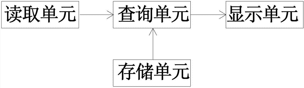
[0042] figure 1 It is a structural schematic diagram of the management system of the wafer acceptance test program according to Embodiment 1 of the present invention; as shown in the figure, the management system of the wafer acceptance test program of Embodiment 1 includes a reading unit, a storage unit, a query unit and display unit;

[0043] Wherein, the product batch number data of several batches of products is stored in the storage unit, and the test machine number data corresponding to the product batch number data of each batch of products, test program name data, probe program name data, probe Card type data, program group name data, machine performance data, copper / non-copper process data, programmer employee number data and test program detailed description data;

[0044] The reading unit obtains an operation data according to the process requirements and transmits the operation data to the query unit; the query unit queries the data information corresponding to th...

Embodiment 2

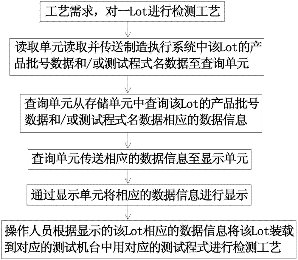
[0048] figure 2 It is a schematic flow chart of the method for applying the management system of the wafer acceptance test program according to Embodiment 2 of the present invention; as shown in the figure, the method of the management system for utilizing the wafer acceptance test program of Embodiment 2 includes the following steps:

[0049] Step 1: When testing a Lot according to production needs, the reading unit reads and transmits the lot number data of the Lot and / or the test program name data of the Lot in the manufacturing execution system to the query unit;

[0050] Step 2: The inquiry unit queries and transmits the data corresponding to the product batch number data of the Lot and / or the test program name data of the Lot stored in the storage unit according to the product batch number data of the Lot and / or the test program name data of the Lot. Data information to the display unit, wherein the corresponding data information includes: the Lot's product batch number...

Embodiment 3

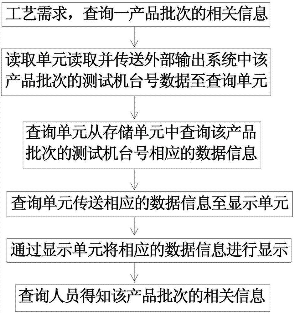
[0053] image 3 It is a schematic flow chart of the method for applying the management system of the wafer acceptance test program according to embodiment 3 of the present invention; as shown in the figure, the method for utilizing the management system of the wafer acceptance test program of embodiment 2 includes the following steps:

[0054] Step 1: According to the process requirements, the reading unit reads and transmits the test machine number data of a batch of products from an external output system to the query unit;

[0055] Step 2: The query unit queries and transmits the data information corresponding to the test machine number data stored in the storage unit to the query unit according to the test machine number data of the batch of products, wherein the corresponding data information includes: The product batch number data of the batch of products, the test machine number data of the batch of products, the test program name data of the batch of products, the prob...


PUM


Abstract

The invention relates to a management system of a wafer acceptable test procedure and an application method of the management system. The management system of the wafer acceptable test procedure comprises a reading unit, a storage unit, an inquiry unit and a display unit. The storage unit is provided with product lot number data of a plurality of batches of products, testing machine number data, testing procedure name data, probe procedure name data, probe card type data, procedure grouping name data, machine property data, copper/non-copper wiring data, procedure establishing personnel job number data and test procedure detailed description data, wherein the testing machine number data, the testing procedure name data, the probe procedure name data, the probe card type data, the procedure grouping name data, the machine property data, the copper/non-copper wiring data, the procedure establishing personnel job number data and the test procedure detailed description data correspond to the product lot identification numbers of the various batches of products. The reading unit obtains operational data as required and transmits the operational data to the inquiry unit. The inquiry unit inquires data information which is stored in the storage unit and corresponds to the operational data and the corresponding data information is displayed through the display unit. According to the management system of the wafer acceptable test procedure and the application method, an operator is enabled to be clear about the fact that the wafer acceptable test procedure is carried out in a corresponding testing machine, testing efficiency is improved, and the factory cost of semiconductors is reduced.

Description

technical field [0001] The invention relates to the field of semiconductor manufacturing, in particular to a wafer acceptance test program management system and an application method thereof. Background technique [0002] In the semiconductor manufacturing process, it is necessary to go through hundreds of process steps before the semiconductor device can be prepared on the wafer. Due to the complexity of the process steps, it is necessary to perform a Wafer Acceptance Test (WAT) on each wafer. And indispensable. In semiconductor manufacturing, test efficiency is an important part of cost management. The higher the test efficiency, the faster the delivery time of semiconductor devices, and the lower the cost of semiconductors. [0003] However, since semiconductor factories produce many different types of products in each period of time, the procedures for wafer acceptance testing for each type of product are different, and the machines that can be used for testing are also...

Claims


Application Information

Patent Timeline
Patent Type & Authority Applications(China)
IPC IPC(8): H01L21/67H01L21/66
Inventor 徐燕菁莫保章娄晓祺
Owner SHANGHAI HUALI MICROELECTRONICS CORP
Why Eureka
Try Eureka