
Single-layer multi-point capacitive touch screen

A capacitive touch screen, single-layer multi-point technology, applied in electrical digital data processing, instruments, data processing input/output process and other directions, can solve the problems of high ITO square resistance, inability to carry out medium and large size structures, etc.

Active Publication Date: 2016-08-10
ANHUI JINGZHUO OPTICAL DISPLAY TECH CO LTD
View PDF9 Cites 0 Cited by
  • Summary
  • Abstract
  • Description
  • Claims
  • Application Information

AI Technical Summary

Problems solved by technology

[0004] The above-mentioned single-layer multi-point design needs to use relatively narrow ITO as the lead in the visible area of ​​the touch screen, but due to the relatively high square resistance of ITO (100-500Ω), usually only 5 inches and 5 inches can be achieved. inch or less, medium and large size structures cannot be carried out

Method used


Image

  • Single-layer multi-point capacitive touch screen
  • Single-layer multi-point capacitive touch screen
  • Single-layer multi-point capacitive touch screen

Examples


Embodiment Construction

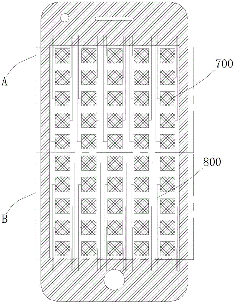
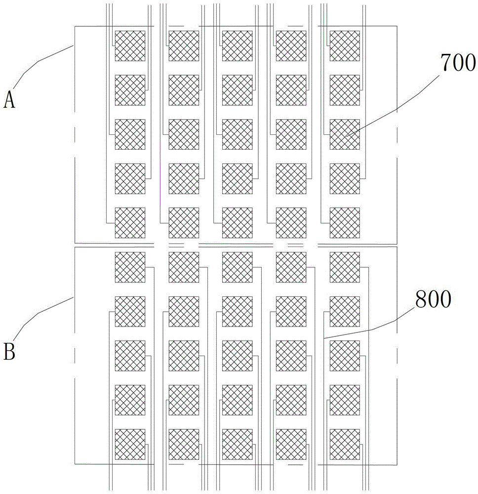
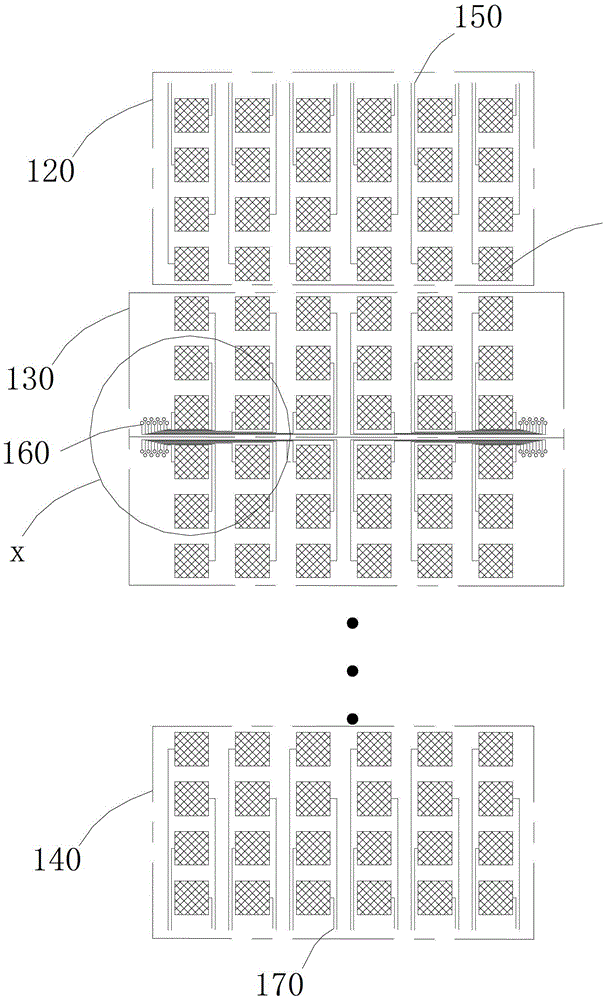
[0027] Please refer to image 3 and Figure 4 , shows a schematic diagram of a wiring structure of a single-layer multi-point capacitive touch screen of an embodiment. The single-layer multi-point capacitive touch screen is provided with a visible area, outside the visible area is the non-visible area of ​​the touch screen, that is, the frame of the touch screen, and the non-visible area can generally be divided into the first end non-visible area (usually That is, the top non-visible area), the second end non-visible area (ie, the bottom non-visible area) and the side non-visible area are well known to those skilled in the art and will not be repeated here. Such as image 3 As shown, the visible area of ​​the single-layer multi-point capacitive touch screen is formed by a plurality of independent electrode units 110 arrayed in multiple rows and columns, wherein each of the plurality of electrode units 110 has wires drawn out.

[0028] Such as image 3 As shown, the visibl...


PUM


Abstract

The invention relates to a monolayer multipoint capacitive touch screen which comprises a touch panel with a visible area. A plurality of independent multi-line multi-column electrode units are arranged in the visible area and the visible area comprises a first end visible area, a second end visible area and a middle visible area. The electrode units in the first end visible area are connected to a first end non-visible area through independent first lines; the electrode units in the middle visible area are connected to a side edge non-visible area through independent middle lines; and the electrode units in the second end visible area are connected to a second end non-visible area through independent second lines. In the side edge non-visible area, the middle lines are connected to the first end non-visible area through a second conducting wire; and in the second end non-visible area, the second lines are connected with and penetrate through the side edge non-visible area through a third conducting wire and then are connected to the first end non-visible area. Line lengths of the middle visible area are short, a resistance value of a whole sensing channel is reduced, and medium and large dimensions can be supported.

Description

technical field [0001] The invention relates to the field of touch control, in particular to a single-layer multi-point capacitive touch screen. Background technique [0002] Common touch panel components usually include one or more layers of electrodes for transmitting / sensing signals, a substrate for supporting the electrodes, a shielding component and another substrate with scratch resistance, anti-glare, anti-fingerprint / water, anti-reflection, etc. Manufacturing such touch panels requires bonding two separately fabricated components together. If a two-layer substrate with a substrate containing multi-layer sensing electrode units plus another substrate with a shielding component and a substrate with scratch resistance, anti-glare, anti-fingerprint / water, anti-reflection, etc. is used, the thickness of the touch panel will be relatively large. Thick and multi-layer sensing electrode unit substrates need to be fabricated in layers and combined together, the production pr...

Claims


Application Information

Patent Timeline
Patent Type & Authority Patents(China)
IPC IPC(8): G06F3/044
Inventor 梁正刚
Owner ANHUI JINGZHUO OPTICAL DISPLAY TECH CO LTD
Learn More