A chamfering grinding wheel and chamfering method for processing thick-layer epitaxial silicon single wafer

A silicon single wafer and chamfering technology, which is used in metal processing equipment, machine tools suitable for grinding workpiece edges, manufacturing tools, etc., can solve the problems of rough edges of silicon single wafers and failure to completely eliminate the rough shape of rough chamfers. , to achieve the effect of good edge quality consistency, elimination of adverse effects, and high edge contour accuracy

Active Publication Date: 2015-07-29
CHINA ELECTRONICS TECH GRP NO 46 RES INST
View PDF15 Cites 0 Cited by
  • Summary
  • Abstract
  • Description
  • Claims
  • Application Information

AI Technical Summary

Problems solved by technology

However, the existing chamfering methods cannot meet the needs of silicon substrates for thick-layer epitaxial growth. There are local rough areas on the edge

Method used


Image

  • A chamfering grinding wheel and chamfering method for processing thick-layer epitaxial silicon single wafer
  • A chamfering grinding wheel and chamfering method for processing thick-layer epitaxial silicon single wafer
  • A chamfering grinding wheel and chamfering method for processing thick-layer epitaxial silicon single wafer

Examples


Embodiment Construction

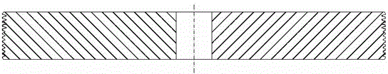
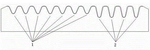
[0016] The present invention will be further explained below with reference to the drawings and embodiments: figure 1 with figure 2 In this embodiment, the rough-chamfered grinding wheel groove and the fine-chamfered grinding wheel groove are made on the same chamfered grinding wheel (the rough-chamfered grinding wheel and the fine-chamfered grinding wheel can also be made respectively). The chamfered grinding wheel contains seven rough chamfers. Grinding wheel groove 1 and four fine chamfering grinding wheel grooves 2, the chamfering grinding wheel is installed on the main shaft of the chamfering machine through the shaft hole, the chamfering machine is a general equipment in the industry.

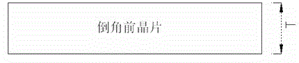
[0017] image 3 For the shape of the silicon single wafer before chamfering, it can be seen that the edge of the silicon single wafer is a right-angled structure before chamfering, which is prone to chipping. Therefore, the edge of the silicon single wafer must be chamfered.

[0018] Reference...


PUM

PropertyMeasurementUnit
particle sizeaaaaaaaaaa

Abstract

The invention relates to a chamfering grinding wheel for machining a silicon single crystal wafer for thick-layer epitaxy, and a chamfering method. The diameters of coarse chamfering grooves of the grinding wheel are 120-150 micrometers less than the thickness of the wafer; half angles are 18-22 degrees; the depths are 900-1100 micrometers; the diamond sizes are 600-1000#; the diameters of fine chamfering grooves are 160-180 micrometers less than the thickness of the wafer; half angles are 11 degrees; the depths are 1400-1600 micrometers; the diamond sizes are 1000-2000#; the rotating speed of the coarse chamfering grinding wheel is 2500-5000rpm; machining is conducted for 1-2 rings; the rotating speed of the wafer is 16-20mm / s; the rotating speed of the fine chamfering grinding wheel is 3000-5000rmp; machining is conducted for 2-4 rings; and the rotating speed of the wafer is 10-15mm / s. The edge chamfering is conducted on the wafer by adopting the chamfering grinding wheel, so that the accuracy of an edge contour is high, the consistency of the edge quality is good, and the problem of a slip line due to the defect of the edge of the silicon wafer in a growth process of the thick-layer epitaxy is solved effectively.

Description

Technical field [0001] The invention relates to the processing of silicon single wafers, in particular to a chamfering grinding wheel and a chamfering method for processing silicon single wafers for thick epitaxy. Background technique [0002] In VDMOS, IGBT and other power electronic devices, silicon single wafers for thick epitaxy are often used as key raw materials. In the thick epitaxial growth of a silicon single wafer, the edge is particularly prone to "epitaxial crown" or slip line defects, which will have adverse effects on subsequent applications. [0003] The edge defects of thick epitaxy are mainly caused by the edge quality of silicon wafers. On the one hand, due to the crystal orientation, the edge of the silicon wafer has a higher deposition rate than the surface of the silicon wafer during epitaxial growth. If the surface of the silicon wafer edge is too small or the angle is too large, it is easy to form extrusion at the edge The stress, and this stress increases ...

Claims


Application Information

Patent Timeline
Patent Type & Authority Patents(China)
IPC IPC(8): B24B9/16
Inventor 张伟才陶术鹤陈建跃康洪亮赵权
Owner CHINA ELECTRONICS TECH GRP NO 46 RES INST
Why Eureka
Try Eureka