

Micro LED array device for display and lighting and preparation method
An LED array, miniature technology, applied in the direction of electric solid-state devices, semiconductor devices, electrical components, etc., can solve problems such as inability to adapt to needs, difficulty in reducing the size of light-emitting units, and resolution limitations.
- Summary
- Abstract
- Description
- Claims
- Application Information
AI Technical Summary
Problems solved by technology
Method used
Image

Examples
specific Embodiment approach 1
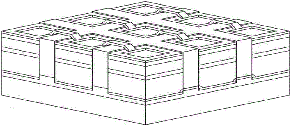
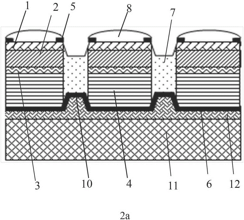
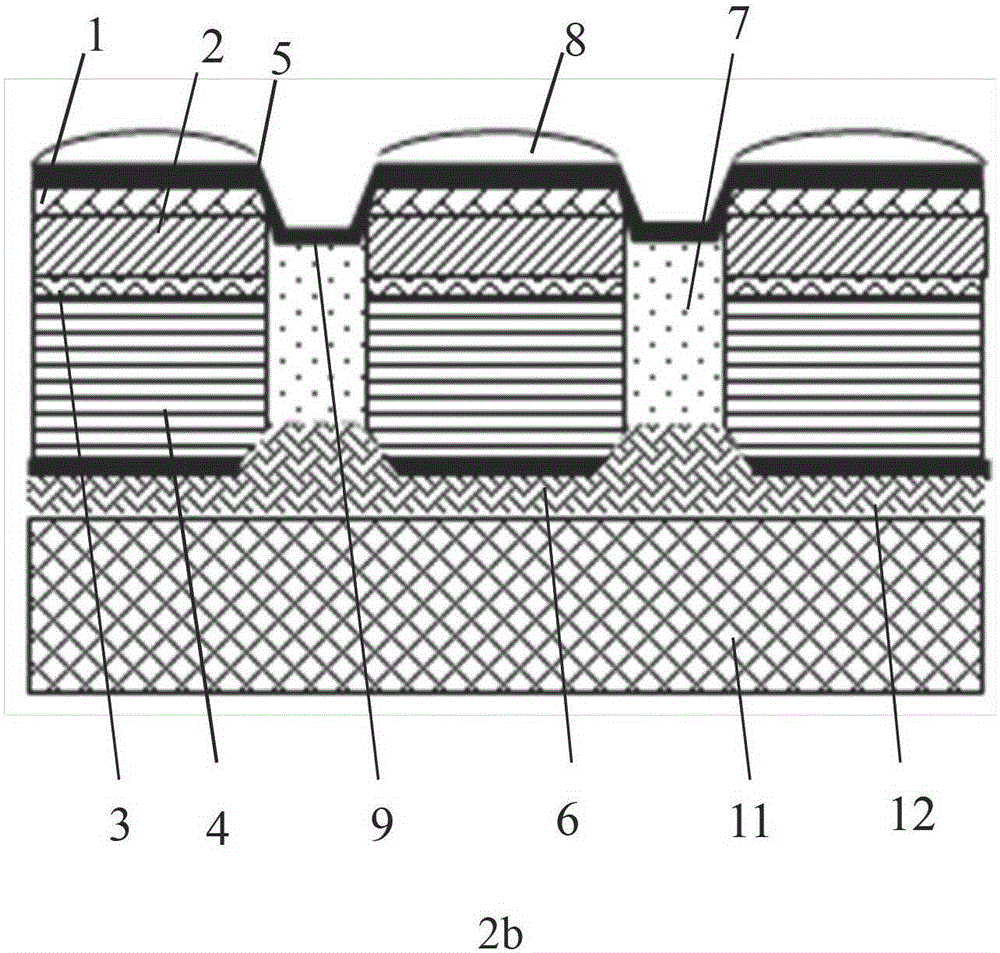
[0027] Specific implementation mode 1. Combination Figure 1 to Figure 8 Describe this embodiment mode; the micro-LED array device for display and illumination described in this embodiment mode includes: a light-transmitting layer 1, a light-emitting layer 2, a reflective layer 3, a substrate 4, an upper electrode 5, an upper electrode lead 9, Lower electrode 6 , lower electrode leads 10 , diaphragm 7 , microlens 8 , adhesive material 12 and substrate 11 .
[0028] The light-transmitting layer 1, the light-emitting layer 2, the reflective layer 3, the substrate 4 and the micro-lens 8 form a square or rectangular or circular or other shaped LED light-emitting unit. The upper surface of the reflective layer 3 is the luminous layer 2 , the light-transmissive layer 1 and the microlens 8 in sequence, and the lower surface of the reflective layer 3 is the substrate 4 . The LED light-emitting units are uniformly arranged to form a light-emitting unit array. Between the light-emitti...
specific Embodiment approach 2
[0031] Specific embodiment two, combine Figure 9 Describe this embodiment mode, this embodiment mode is the manufacturing method of the micro-LED array device used for display and lighting described in the first specific embodiment mode, this embodiment mode adopts a top-down manufacturing method, that is, the front structure is fabricated first, and then , then protect the front structure and prepare the back structure; the specific process is:
[0032] A. Cleaning and front protection of light-emitting chips:
[0033]a) The substrate material used in this embodiment is a light-emitting chip, and the light-emitting chip used is composed of a light-transmitting layer, a light-emitting layer, a reflective layer and a substrate, such as Figure 9 as shown in a.
[0034] b) Cleaning the light-emitting chip. Then prepare a layer of protective film on the upper surface of the light-emitting chip, that is, the upper surface of the light-transmitting layer, such as Figure 9 as ...
specific Embodiment approach 3
[0060] Specific Embodiment 3. This embodiment is an example of the method for preparing a micro-LED array device for display and lighting described in Specific Embodiment 2:
[0061] 1. Cleaning and front protection of light-emitting chips:
[0062] a. The light-emitting chip used in the present invention is an AlGaInP-LED epitaxial wafer, which is composed of a light-transmitting layer, a light-emitting layer, a reflective layer and a substrate, and the thickness of the light-emitting chip is 200 μm to 1000 μm.
[0063] b. The material of the upper protective film is silicon dioxide or silicon nitride or a composite film composed of silicon dioxide and silicon nitride or metal or organic material or inorganic material or other film materials that can play a protective role. The preparation method of the protective film is electron beam evaporation, radio frequency sputtering, magnetron sputtering, sol-gel method or other film growth methods.
[0064] 2. Preparation of the up...
PUM
 Abstract
Description
Claims
Application Information