Non-rectangular display apparatus

A display device, non-rectangular technology, applied in nonlinear optics, static indicators, optics, etc., can solve the problem of not mentioning the positional relationship of the gate line and data line liquid crystal drive circuit, etc., to achieve large and small effects

Active Publication Date: 2014-01-01
TIANMA MICRO ELECTRONICS CO LTD
View PDF6 Cites 36 Cited by
  • Summary
  • Abstract
  • Description
  • Claims
  • Application Information

AI Technical Summary

Problems solved by technology

[0022] However, there is no mention of the positional relationship between the gate lines and data lines that make up the liquid crystal panel and the liquid crystal drive circuit that drives them.

Method used


Image

  • Non-rectangular display apparatus
  • Non-rectangular display apparatus
  • Non-rectangular display apparatus

Examples


no. 1 Embodiment approach

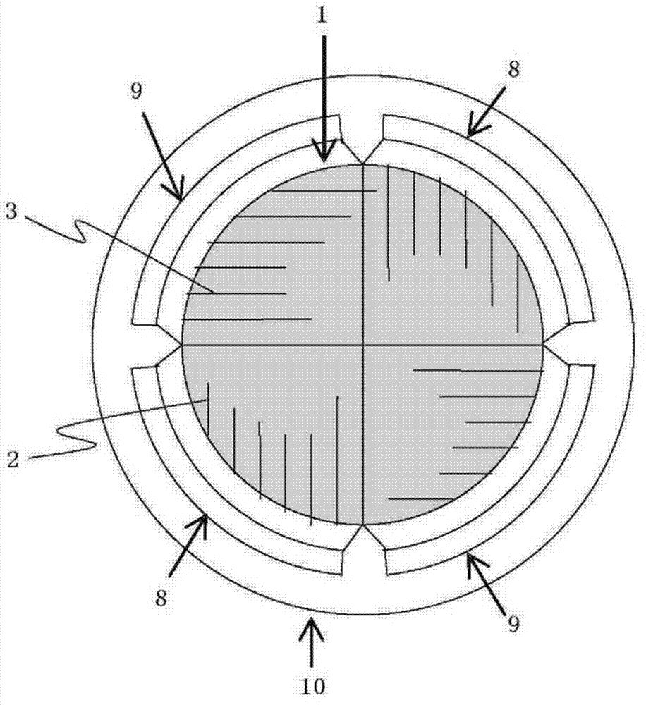
[0113] figure 1 It is a figure which shows the structure of an embodiment of this invention. The display unit 1 is a non-rectangular display device that is circular. The display device of this embodiment includes an active matrix display portion formed on a display substrate 10 and composed of a plurality of scanning lines 2, a plurality of signal lines 3, and thin film transistors 4 as pixels and active elements arranged at the intersections thereof 1, and, for example, two scanning line drive circuits 8 and two signal line drive circuits 9 composed of thin film transistors.

[0114] Here, the planar shapes of the scanning line driver circuit 8 and the signal line driver circuit 9 are fan-shaped, and they are bent along the outer periphery of the display unit 1, so that the shape of the display substrate 10 can be made as compared with the non-rectangular display unit 1. Similar in shape, the size of the display portion 1 is close to the size of the display substrate 10, and a...

no. 2 Embodiment approach

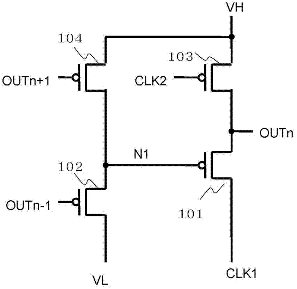
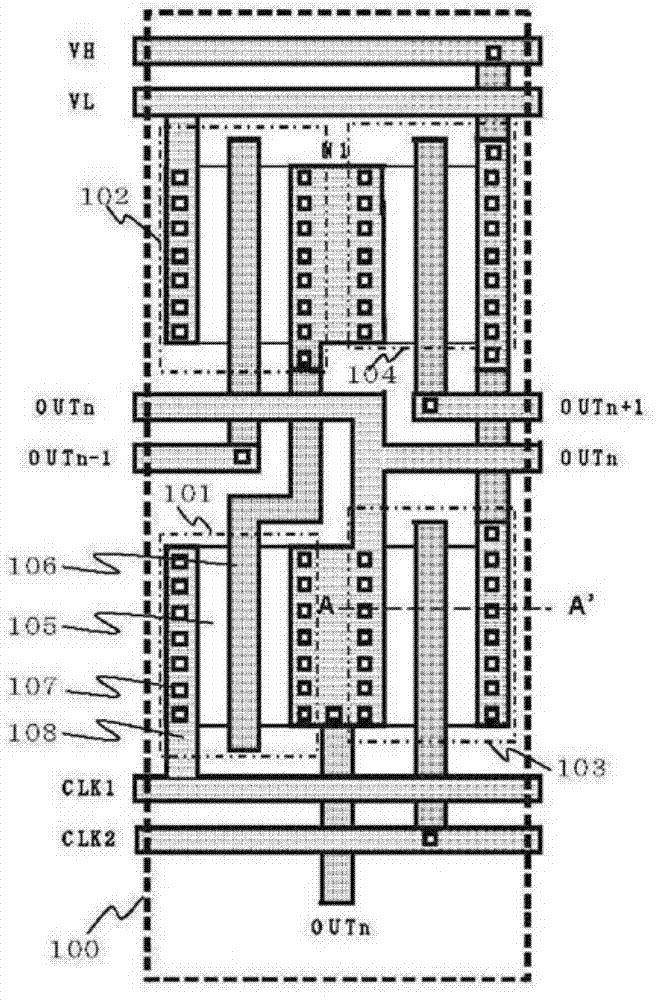
[0155] Picture 9 It is a diagram showing the layout of the second embodiment of the present invention. In this embodiment, except Figure 7 In addition to repeated parallel movement in the X and Y directions, each shift register 100 is tilted at any angle.

[0156] In this way, the shift registers 100 can be arranged near the periphery of the display portion. In addition, the power supply lines VH and VL and the clock signal wirings CLK1, CLK2 and the mutual output wiring are connected between the shift registers 100 in the shortest manner, for example, obliquely.

[0157] In this embodiment, between the shift registers 100, the interval in the X direction is equal to the interval between the scanning lines 2 and is constant, while the interval in the Y direction and the pitch of the rotation angle are variable.

[0158] By arbitrarily determining the last two points, the distance between the shift registers 100 can be adjusted between the shift registers 100, that is, the distance...

no. 3 Embodiment approach

[0161] Picture 10 It is a figure which shows an example of the layout of the 3rd Embodiment of this invention. In this embodiment, the pitch of each shift register with an arbitrary angle along the outer periphery of the display unit 1 is made narrower.

[0162] That is, the layout of the rectangular shift register 100 ( image 3 The bottom corners of) are approached in a manner of contact between adjacent shift registers 100. In this way, the length of the entire scanning line driving circuit 8 can be shortened.

[0163] Furthermore, on the outer periphery of the display unit 1, if the scanning line drive circuit 8 of this embodiment occupies the Figure 7 , Picture 9 With the same length, the layout width of each shift register 100 can be increased.

[0164] If the circuit scale is the same, correspondingly, the layout height of the shift register 100 can be reduced. This means that the width of the scanning line driving circuit 8 becomes smaller, and a display device with a na...


PUM


Abstract

Disclosed is a display apparatus comprising an active matrix display section including a plurality of signal lines and scan lines, arranged in a matrix on a substrate, and a plurality of pixels and active elements arranged at intersections of the signal and scan lines, a scan line driving circuit for driving the scan lines and a signal line driving circuit for driving the signal lines. The display section has a non-rectangular shape. The active elements that make up the scan line driving circuit and / or the signal line driving circuit are formed by the same manufacturing process as that for forming the active elements in the active matrix display section. The scan line driving circuit and / or the signal line driving circuit are each a set of circuit units having the same function.; These circuit units are arranged to conform to and extend around the outer circumference of the non-rectangular display section.

Description

[0001] This application is a divisional application of the application whose application date is April 28, 2008, the application number is 200810092390.4, and the invention title is "non-rectangular display device". Technical field [0002] The present invention relates to a display device in which the display portion has a non-rectangular shape. Background technique [0003] Figure 24 It is a diagram showing a typical configuration of a conventional active matrix display device. Such as Figure 24 As shown, pixels and active elements, such as thin film transistors, are provided at intersections of signal lines and scanning lines arranged in a matrix. While the selection pulse is input to one scan line, the active element connected to the gate terminal of the scan line is turned on, and the signal potential charged on the signal line is applied to the pixel, such as liquid crystal. Due to this potential, the optical properties of the liquid crystal material will change, which can ...

Claims


Application Information

Patent Timeline
Patent Type & Authority Applications(China)
IPC IPC(8): G02F1/133G02F1/1362G09G3/36
CPCH10K59/131
Inventor 野中义弘
Owner TIANMA MICRO ELECTRONICS CO LTD
Why Eureka
Try Eureka