A detection method for layout design photolithography process friendliness

A technology of lithography process and detection method, which is applied in the direction of photolithography exposure device, micro-lithography exposure equipment, etc., can solve the problem of high production cost, long software calculation and use time, unfavorable layout design, lithography process friendliness detection kit Application and other issues to achieve the effect of improving production efficiency, reducing software calculation and use time, and reducing production costs

Active Publication Date: 2015-11-25
SHANGHAI HUALI MICROELECTRONICS CORP
View PDF5 Cites 1 Cited by
  • Summary
  • Abstract
  • Description
  • Claims
  • Application Information

AI Technical Summary

Problems solved by technology

Although this method can accurately find process hotspots, the software calculation and use time of the whole process will be very long, and the corresponding production costs will be relatively high, and it is not conducive to the foundry's layout design photolithography process friendliness detection kit in the design company application

Method used


Image

  • A detection method for layout design photolithography process friendliness
  • A detection method for layout design photolithography process friendliness
  • A detection method for layout design photolithography process friendliness

Examples


Embodiment Construction

[0030] Some typical embodiments embodying the features and advantages of the present invention will be described in detail in the following description. It should be understood that the present invention can have various changes in different examples, which do not depart from the scope of the present invention, and the descriptions and diagrams therein are essentially for illustrative purposes rather than limiting the present invention.

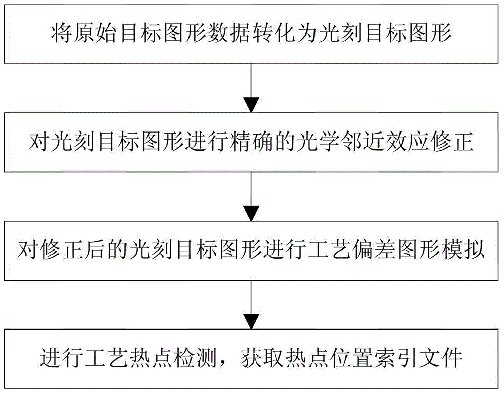
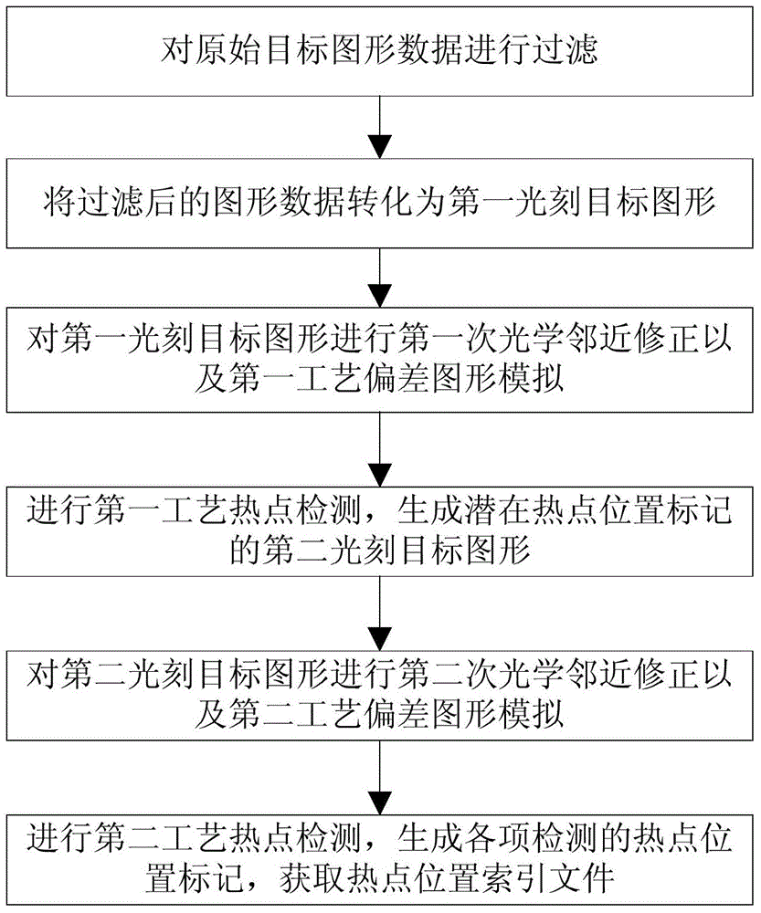
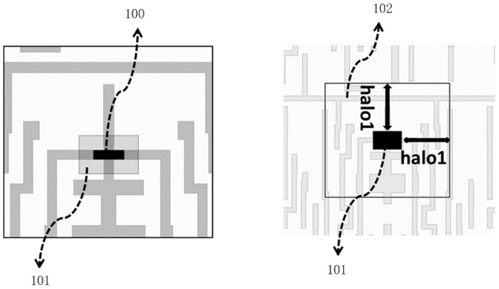
[0031] The above and other technical features and beneficial effects will be combined with Figure 2-4 with Figure 5a~5f A preferred embodiment of the method for detecting the friendliness of the layout design lithography process of the present invention will be described in detail.

[0032] figure 2 It is a schematic flow diagram of a specific embodiment of the method for detecting the friendliness of the layout design lithography process of the present invention. The following specifically describes the method for detecting the friendliness of...


PUM


Abstract

The invention discloses a layout design photolithographic technology friendliness detection method which comprises the steps of filtering original target graphic data in advance to determine a latent technology hot spot region, converting the graphic data of the latent technology hot spot region into photolithographic target graphic data, then performing simplified optical proximity correction and graphic simulation on the photolithographic target graphic data to preliminarily investigate technology hot spots, and performing precise and complete optical proximity correction and precise and complete graphic simulation according to a technology hot spot preliminary investigation labeled position and graphic data of necessary surrounding positions to execute final check on the technology hot spots. Therefore, on the premise that the technology hot spots are precisely found, the software calculation time and the software use time are shortened in the whole process, the production cost is reduced, and the production efficiency is improved.

Description

Technical field [0001] The invention relates to the field of manufacturability graphic design (DesignForManufacture, DFM), and in particular to a method for detecting the friendliness of a layout design photoetching process. Background technique [0002] In the integrated circuit manufacturing process, in order to smoothly transfer the pattern of the integrated circuit to the wafer, a mask is first made according to the designed layout, and then the pattern on the mask is transferred to the wafer by photolithography technology Above, due to the influence of optical proximity effect (Optical Proximity Effect, OPE) in sub-wavelength lithography technology, when the high-density array of mask circuit patterns are exposed and finally transferred to the wafer, greater distortion will occur, such as Right-angled corner rounded (right-angled corner rounded), line end shortened (lineend shortened), and line width increase / decrease (linewidth increase / decrease) are common optical proximit...

Claims


Application Information

Patent Timeline
Patent Type & Authority Patents(China)
IPC IPC(8): G03F7/20
Inventor 王伟斌阚欢魏芳张旭昇
Owner SHANGHAI HUALI MICROELECTRONICS CORP
Why Eureka
Try Eureka