Electronic element mounting device and electronic element mounting method

An electronic component installation and electronic component technology, applied in the direction of electrical components, electrical components, etc., can solve the problem of wasting time in the component installation mechanism, and achieve the effect of eliminating wasted time and improving the efficiency of installation work.

Inactive Publication Date: 2014-05-21
PANASONIC INTELLECTUAL PROPERTY MANAGEMENT CO LTD
View PDF5 Cites 2 Cited by
  • Summary
  • Abstract
  • Description
  • Claims
  • Application Information

AI Technical Summary

Problems solved by technology

Therefore, during the period until the positioning operation accompanying the board movement is completed, the component mounting mechanism wastes time in a state of standby in an operation stop state, which becomes a constraint in improving the efficiency of mounting work.

Method used


Image

  • Electronic element mounting device and electronic element mounting method
  • Electronic element mounting device and electronic element mounting method
  • Electronic element mounting device and electronic element mounting method

Examples


Embodiment Construction

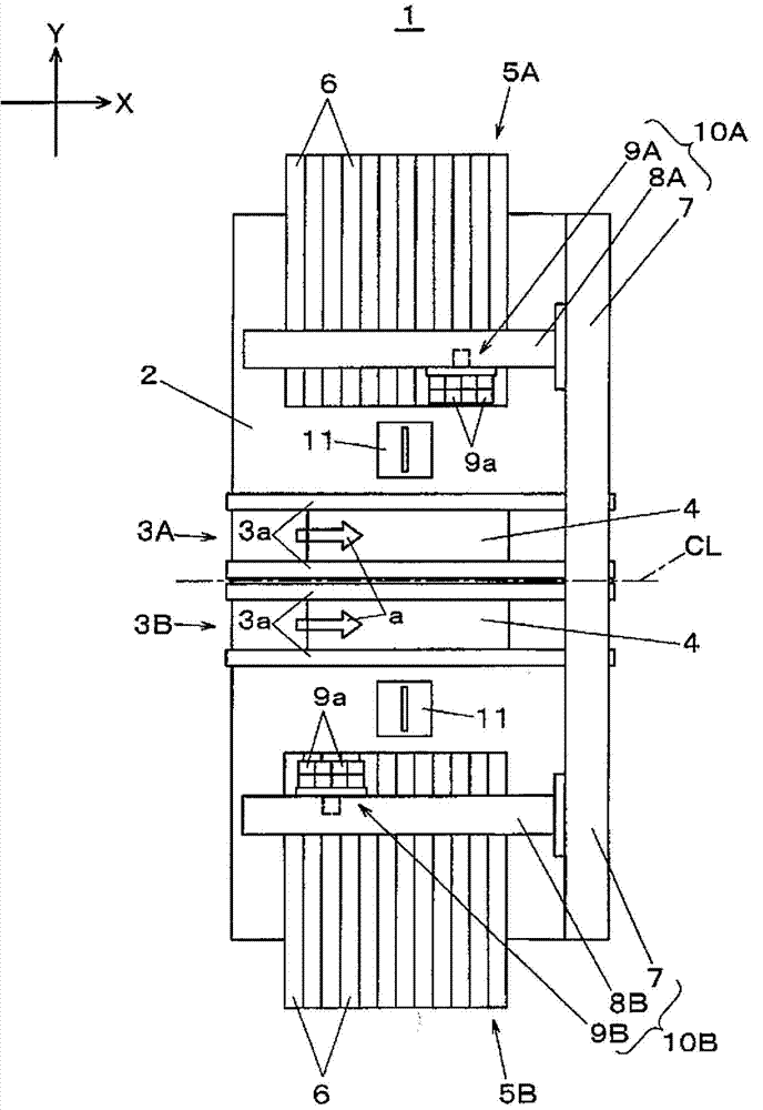
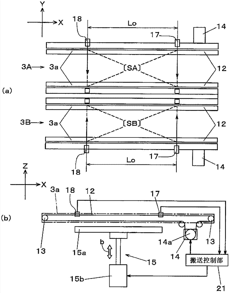
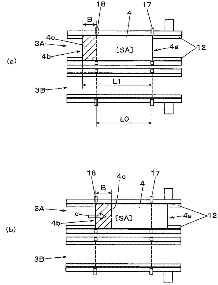
[0032] Hereinafter, embodiments of the present invention will be described with reference to the drawings. First, refer to figure 1 , the structure of the electronic component mounting apparatus 1 will be described. exist figure 1 In the center of the base 2 , a first substrate conveyance mechanism 3A and a second substrate conveyance mechanism 3B are arranged side by side across the apparatus center line CL. The first substrate conveyance mechanism 3A and the second substrate conveyance mechanism 3B each have two conveyance rails 3a, receive the substrate 4 to be mounted from the upstream side (see arrow a), convey and position it in the X direction (substrate conveyance direction) .

[0033] A first component supply unit 5A and a second component supply unit 5B are arranged outside the first substrate transport mechanism 3A and the second substrate transport mechanism 3B, respectively, and the first component supply unit 5A and the second component supply unit 5B are arra...


PUM


Abstract

The invention aims to provide an electronic element mounting device and an electronic element mounting method, wherein wasted time in standby of an element mounting mechanism in an action stoppage state can be eliminated, and mounting operation efficiency is improved. A positioning holding part which is arranged on a substrate conveying mechanism is utilized for successively positioning and holding the substrate to a plurality of mounting operation positions. In one substrate conveying mechanism, in the process of successively performing element mounting operation at each element mounting position, if substrate positioning finishing is detected in another substrate conveying mechanism at the time when element mounting operation at one mounting operation position is finished, element mounting operation is performed on the substrate of which positioning finishing is detected in another substrate conveying mechanism before one substrate conveying mechanism begins the element mounting operation at a subsequent mounting operation position of one mounting operation position in one substrate conveying mechanism.

Description

technical field [0001] The present invention relates to an electronic component mounting device and an electronic component mounting method for mounting electronic components on a substrate. Background technique [0002] In an electronic component mounting apparatus that mounts electronic components on a substrate to manufacture a mounting substrate, a substrate conveying mechanism for conveying the substrate from the upstream side to the downstream side is provided, so that the substrate is conveyed by the substrate conveying mechanism and positioned at a predetermined mounting operation position. The substrate is used as the target, and the component mounting operation is carried out by using the mounting head of the component mounting mechanism to transport and mount the electronic components taken out from the component supply unit. In this component mounting work, the movable range of the mounting head is not limited to the range that can cover the entire substrate to b...

Claims


Application Information

Patent Timeline
Patent Type & Authority Applications(China)
IPC IPC(8): H05K13/04
Inventor 山崎琢也竹原裕起相良博喜粟田义明
Owner PANASONIC INTELLECTUAL PROPERTY MANAGEMENT CO LTD
Why Eureka
Try Eureka