

Transparent waveguide display
A technology of a waveguide layer and a waveguide device, applied in the field of transparent waveguide display devices, can solve problems such as low efficiency and limitation
Active Publication Date: 2014-05-28
ROCKWELL COLLINS INC +1
View PDF19 Cites 134 Cited by
- Summary
- Abstract
- Description
- Claims
- Application Information
AI Technical Summary
Problems solved by technology
While the tiling disclosed in this earlier document overcomes the twin drawbacks of standard guided wave structures: limited field of view and limited pixel resolution, it has limitations when it is necessary to til
Method used
View moreImage
Smart ImageViewing Examples

Examples
 PUM
| Property | Measurement | Unit |
|---|---|---|
| Thickness | aaaaa | aaaaa |
Abstract
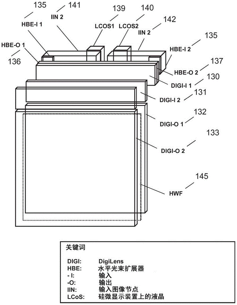
One embodiment provides an apparatus for displaying an image comprising: a first optical substrate comprising at least one waveguide layer configured to propagate light in a first direction, wherein the at least one waveguide layer of the first optical substrate comprises at least one grating lamina configured to extract the light from the first substrate along the first direction; and a second optical substrate comprising at least one waveguide layer configured to propagate the light in a second direction, wherein the at least one waveguide layer of the second optical substrate comprises at least one grating lamina configured to extract light from the second substrate along the second direction; and the at least one grating lamina of at least one of the first and second optical substrates comprises an SBG in a passive mode.
Description
[0001] related application [0002] This application is a continuation-in-part of U.S. Application No. 13 / 844456, filed March 15, 2013, which requires U.S. Provisional Application No. 61 / 796,632, filed November 16, 2012 and February 2013 Priority to US Provisional Application No. 61 / 849,853 filed on 4th, each of which is hereby incorporated by reference in its entirety. technical field [0003] This application relates to a transparent waveguide display device Background technique [0004] There is a need for a compact transparent data display device capable of displaying image content ranging from symbolic and alphanumeric arrays to high resolution pixelated images. Examples of transparent display devices include HMDs, HUDs, HDDs and others. In each case, an important element is that the display device should be highly transparent and the displayed image content should be clearly visible when placed on a bright background. The display device should provide full color wit...
Claims
Login to View More Application Information
Patent Timeline
 IPC IPC(8): G02B5/18G02B5/32G02B27/01
CPCG02B5/1814G02B27/4272G02B27/0172G02B2027/0118G02B6/0013G03H2260/34G02F1/29
InventorR·D·布朗A·J·格兰特W·L·亨德里克M·M·波波维奇J·H·斯坦利J·D·瓦尔德恩
OwnerROCKWELL COLLINS INC