Integrated circuit having gates and active regions forming a regular grating

a technology of integrated circuits and active regions, applied in the field of semiconductor devices, can solve the problems of reducing the yield and/or stability of devices, increasing the difficulty of fabricating complex geometries in ic devices, and posing significant challenges, so as to facilitate the introduction of new high-resolution patterning technologies, improve the controllability of critical device dimensions, and improve the resolution and controllability

Inactive Publication Date: 2006-06-08
IBM CORP
View PDF9 Cites 241 Cited by
  • Summary
  • Abstract
  • Description
  • Claims
  • Application Information

AI Technical Summary

Benefits of technology

The present invention provides semiconductor device layout techniques that create periodic gratings in both gates and active regions of the device. These techniques improve resolution and controllability of critical device dimensions by using regular patterns based on fixed line widths and spacings. This also eases lithography constraints and allows for the introduction of new high-resolution patterning technologies. Additionally, self-assembly techniques that can precisely define periodic gratings can be more easily employed with the device layout techniques of the present invention.

Problems solved by technology

The technical problem addressed in this patent text is how to improve the packing density of integrated circuits that contain repeating circuit cells, like SRAM arrays, without compromising their performance and reliability due to process variation during manufacturing. Current methods require complete flexibility in pattern size and orientation, leading to difficulty in achieving optimal results through scaling. A new approach is needed to address this challenge while ensuring efficient production of highly reliable and scalable integrated circuits.

Method used


Image

  • Integrated circuit having gates and active regions forming a regular grating
  • Integrated circuit having gates and active regions forming a regular grating
  • Integrated circuit having gates and active regions forming a regular grating

Examples


Embodiment Construction

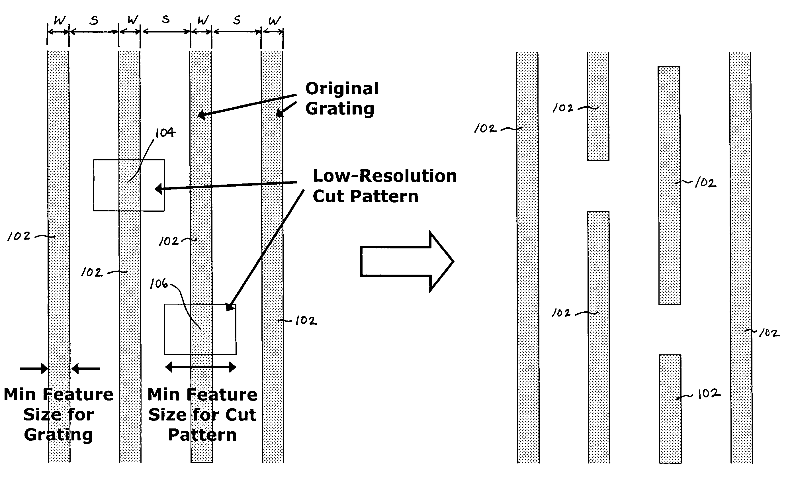
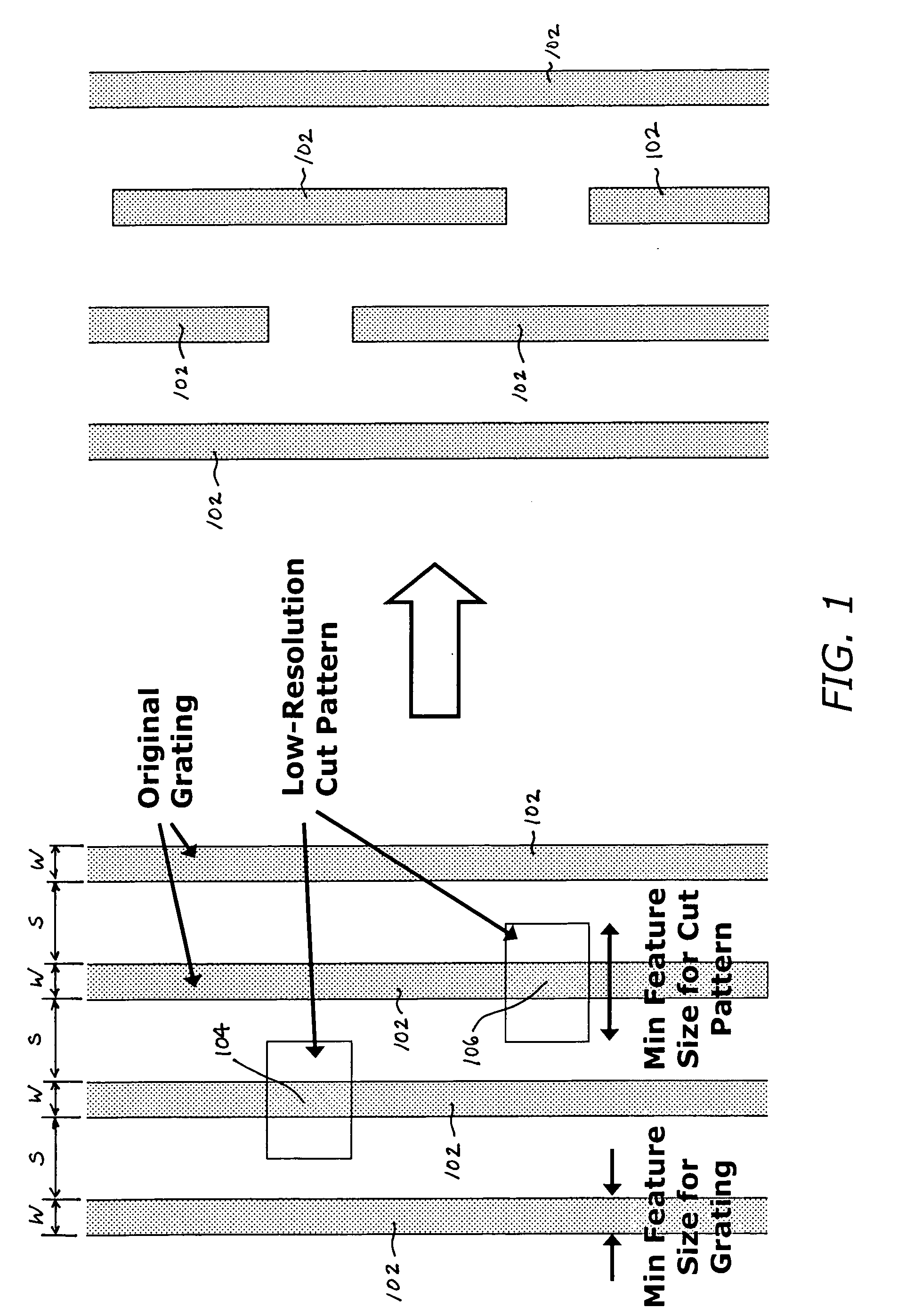
[0020] The present invention will be described herein in the context of an illustrative memory cell for use in an SRAM array comprising a plurality of such memory cells. It should be appreciated, however, that the invention is not limited to this or any particular memory cell configuration. Rather, the invention is more generally applicable to techniques for forming a semiconductor device which may include a plurality of repeated circuit cells, each of the circuit cells being configured such that both gate and active regions in a given layer of the cell form a substantially regular grating. The term “grating” as used herein is intended to refer to a framework of equidistant and parallel lines which may be arranged in a crisscrossed pattern. The term “grating” is often used interchangeably with the term “grid.” In addition to providing increased scalability of the device, thereby beneficially increasing a packing density thereof, the techniques of the present invention described here...


PUM


Abstract

A semiconductor device includes a plurality of repeatable circuit cells connectable to one or more conductors providing at least electrical connection to the circuit cells and/or electrical connection between one or more circuit elements in the cells. Each of the circuit cells are configured having gates and active regions forming a grating, wherein, for a given active layer in the device, a width of each active region is substantially the same relative to one another, a spacing between any two adjacent active regions is substantially the same, a width of each gate is substantially the same relative to one another, and a spacing between any two adjacent gates is substantially the same.

Description


Claims


Application Information

Patent Timeline
Owner IBM CORP
Why Eureka
Try Eureka