TFT array substrate and display device

A technology of array substrates and pixel units, which is applied in the direction of static indicators, instruments, semiconductor devices, etc., can solve the problems of decreased display effect, poor display effect of TFT array substrates and display devices, etc., achieve display brightness balance, improve display quality, The effect of increasing the aperture ratio

Active Publication Date: 2014-07-23
SHANGHAI AVIC OPTOELECTRONICS +1
View PDF6 Cites 16 Cited by
  • Summary
  • Abstract
  • Description
  • Claims
  • Application Information

AI Technical Summary

Problems solved by technology

[0002] Thin Film Transistor (Thin Film Transistor, TFT) array substrates are widely used in display devices, but in actual use, it is found that TFT array substrates and display devices have problems with poor or reduced display effects

Method used


Image

  • TFT array substrate and display device
  • TFT array substrate and display device
  • TFT array substrate and display device

Examples


Embodiment Construction

[0025] In order to make the objectives, technical solutions and advantages of the present invention clearer, the present invention will be further described in detail below in conjunction with the accompanying drawings. Obviously, the described embodiments are only a part of the embodiments of the present invention, rather than all of them. Based on the embodiments of the present invention, all other embodiments obtained by those of ordinary skill in the art without creative work shall fall within the protection scope of the present invention.

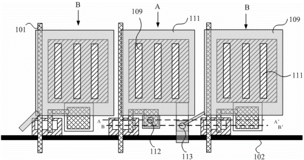
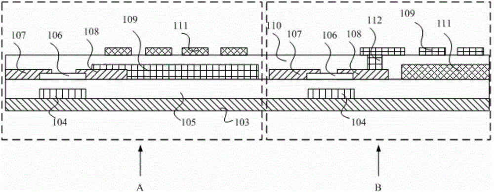
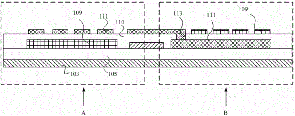
[0026] It should be noted that in the embodiments of the present invention, "top layer" and "bottom layer" only indicate a relative positional relationship between the pixel electrode and the common electrode. For example, the pixel electrode is located on the top layer of the pixel unit, which means that the pixel electrode is located on the common electrode. In the embodiment of the present invention, “row” is not only limited to 1 row o...


PUM


Abstract

The invention discloses a TFT array substrate and a display device. The TFT array substrate comprises a plurality of grid lines and a plurality of data lines, wherein the grid lines and the data lines intersect in an insulating mode and form a plurality of pixel units distributed in an array mode in an enclosure mode. The pixel units comprise drain electrodes, pixel electrodes and common electrodes, wherein the pixel electrodes and the common electrodes form an electric field. The pixel units are divided into the first pixel units and the second pixel units. The electric field directions of every two adjacent pixel units are opposite. According to the TFT array substrate, the display effect and the display quality can be improved.

Description

Technical field [0001] The present invention relates to the field of display technology, in particular to a TFT array substrate and a display device. Background technique [0002] Thin Film Transistor (TFT) array substrates are widely used in display devices. However, in actual use, it has been found that TFT array substrates and display devices have problems with poor display effects or reduced display effects. Summary of the invention [0003] In view of this, embodiments of the present invention provide a TFT array substrate and a display device. [0004] A TFT array substrate includes: a plurality of gate lines and a plurality of data lines, and the gate lines and the data lines are insulated and crossed; the gate lines and the data lines are surrounded to form a plurality of arrays distributed The pixel unit includes a drain, a pixel electrode, and a common electrode, the pixel electrode and the common electrode form an electric field, and the plurality of pixel units includes...

Claims


Application Information

Patent Timeline
Patent Type & Authority Applications(China)
IPC IPC(8): G02F1/1362G02F1/1368G02F1/1343G02F1/13
CPCG09G3/3648G09G3/3614G09G2300/0426G09G2300/0439G09G2300/0478G09G3/3659G09G2300/0809H01L27/124
Inventor 金慧俊林珧
Owner SHANGHAI AVIC OPTOELECTRONICS
Why Eureka
Try Eureka