Scan Test Control Circuit for SoC

A scanning test and control circuit technology, which is applied in the field of system-on-chip, can solve the problems of large dynamic power consumption, etc., and achieve the effects of reducing flipping, improving test pass rate, and reducing IR-drop

Active Publication Date: 2017-07-11
SAMSUNG SEMICON CHINA RES & DEV +1
View PDF4 Cites 0 Cited by
  • Summary
  • Abstract
  • Description
  • Claims
  • Application Information

AI Technical Summary

Problems solved by technology

However, often only a small part of the area needs to be tested, so clock signals and combinational logic change signals are passed to non-test logic, resulting in a large amount of dynamic power consumption and causing IR-Drop problems

Method used


Image

  • Scan Test Control Circuit for SoC
  • Scan Test Control Circuit for SoC
  • Scan Test Control Circuit for SoC

Examples


Embodiment Construction

[0017] The present invention is described more fully hereinafter with reference to the accompanying drawings, in which exemplary embodiments of the invention are shown. However, this invention may be embodied in many different forms and should not be construed as limited to the embodiments set forth herein. Rather, these embodiments are provided so that this disclosure will be thorough and complete, and will fully convey the scope of the invention to those skilled in the art.

[0018] The present invention will be explained in detail with reference to the accompanying drawings.

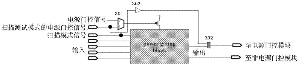
[0019] image 3 is a diagram illustrating a scan test control circuit suitable for an SOC according to an exemplary embodiment of the present invention.

[0020] refer to image 3 , the scan test control circuit suitable for SOC may include an alternative circuit 301 and a shielding circuit 302 , and may optionally include a NOT gate 303 . exist image 3 Only one power-gated module is shown in th...


PUM


Abstract

The invention discloses a sweep test control circuit suitable for a system on chip. The system on chip comprises a plurality of power gating modules and a plurality of non-power-gating modules. The sweep test control circuit comprises a plurality of alternative circuits corresponding to the power gating modules and a plurality of shield circuits, wherein the first input end of each alternative circuit receives a power gating signal, the second input end of each alternative circuit receives a power gating signal in the sweep test mode, the control end of each alternative circuit receives a sweep mode signal, the output end of each alternative circuit is connected to a grid of a gating transistor of the corresponding power gating module, and each shield circuit is connected between the corresponding power gating module and the corresponding non-power-gating module and alternatively outputs 0 or 1.

Description

technical field [0001] The present invention relates to a system on chip (SOC), more specifically, relates to a scanning test control circuit suitable for SOC, and the scanning test control circuit can effectively reduce test power consumption and improve test passing rate. Background technique [0002] As the scale of the system on chip (SOC) becomes larger and larger, due to the consideration of power consumption, the power gating design method is widely used in the field of SOC chip design. At the same time, due to the increase in the scale of the SOC, the requirements for scanning test hardware and software are also getting higher and higher, so group scan testing of SOC chips is becoming more and more popular. [0003] figure 1 is a diagram showing a SOC with power-gated blocks and non-power-gated blocks. refer to figure 1 , P1...Pn represent power-gated modules, N1...Nn represent non-power-gated modules, power-gated modules P1...Pn have gating logic, and arrows repr...

Claims


Application Information

Patent Timeline
Patent Type & Authority Patents(China)
IPC IPC(8): G01R31/28
Inventor 王金城
Owner SAMSUNG SEMICON CHINA RES & DEV
Why Eureka
Try Eureka