This helps you quickly interpret patents by identifying the three key elements:
Problems solved by technology
Method used
Benefits of technology
Problems solved by technology
[0009] However, it is necessary to add a lot of detection capacitors CM in the entire array substrate, and each CM is connected to a detection signal line for signal detection, so that the wiring density on the array substrate becomes larger and the process is increased.
Since each detection capacitor needs to be led out by a detection signal line, there are many detection signal lines when large-scale or high-precision touch is required, so the wiring of the entire display panel will be very difficult, and the detection capacitor will also exist. difference, making it difficult to achieve large-size display panels and high-precision display panels
Method used
Image
Click on the blue label to locate the original text in one second.
Reading with bidirectional positioning of images and text.
Examples
Embodiment 2
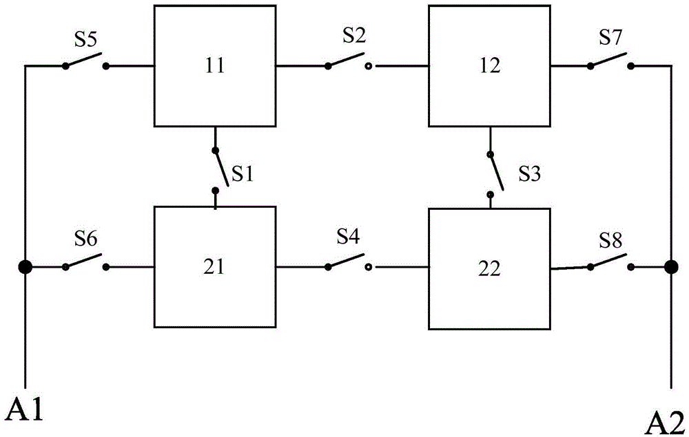
[0070] see Figure 4 , which is a schematic diagram of the corresponding display state of the array substrate provided by the present invention.
[0071] This embodiment introduces the situation when the array substrate corresponds to the display state.
[0072] When the array substrate corresponds to the display state, the first control module is used to control all the first switch units to be turned on; at the same time, the first control module is used to control all the second switch units to be turned off, In order to make the signal line complete the transmission of display data.
[0073] Specific as Figure 4 As shown, all the first switch units S1-S4 are closed, and the corresponding plurality of touch electrodes arranged in an array are electrically connected together, and the normal display function can be completed at this time.
[0074] Since there is no need to perform touch detection at this time, the second switch units S5 - S8 at this time can all be discon...
Embodiment 3
[0086] see Figure 6 , which is a schematic diagram of Embodiment 3 of the array substrate provided by the present invention.
[0087] In this embodiment, the first switch unit includes a first-type switch transistor and the second switch unit includes a second-type switch transistor as an example for introduction.
[0088] In this embodiment, the first type of switching transistor is a PMOS transistor, and the second type of switching transistor is an NMOS transistor as an example for introduction.
[0089] The first control module 601 is also used to generate M pulse driving signals, where M is the number of rows of the touch electrodes; the M driving pulse signals are connected to the gates of the NMOS transistor and the PMOS transistor, and are used to control the NMOS transistor and the gate of the PMOS transistor. The switching state of the PMOS tube.
[0090] Figure 6 Only four rows of touch electrodes are used as an example for illustration, corresponding to four p...
PUM
Abstract
The invention provides an array substrate, a display panel and electronic equipment. The array substrate comprises a touch circuit and a plurality of touch electrodes which are distributed in an arrayed manner, wherein the touch electrodes are insulated from one another; the touch circuit comprises first switch units, second switch units and a first control module; each two adjacent touch electrodes are connected with each other through the corresponding first switch unit; and each touch electrode is connected with a signal line through the corresponding second switch unit. When the array substrate is in a touch detecting state, the first control module is used for controlling the first switch unit to be switched off, and the adjacent touch electrodes are separated from one another one by one; and moreover, the first control module is used for controlling the second switch units to be switched on one by one, and touch detection of all lines of the touch electrodes is finished sequentially. Compared with the prior art, the array substrate has the advantages that a large number of detection signal lines is omitted, circuit wiring of a whole structure is simplified, wiring space is saved, and the cost is reduced.
Description
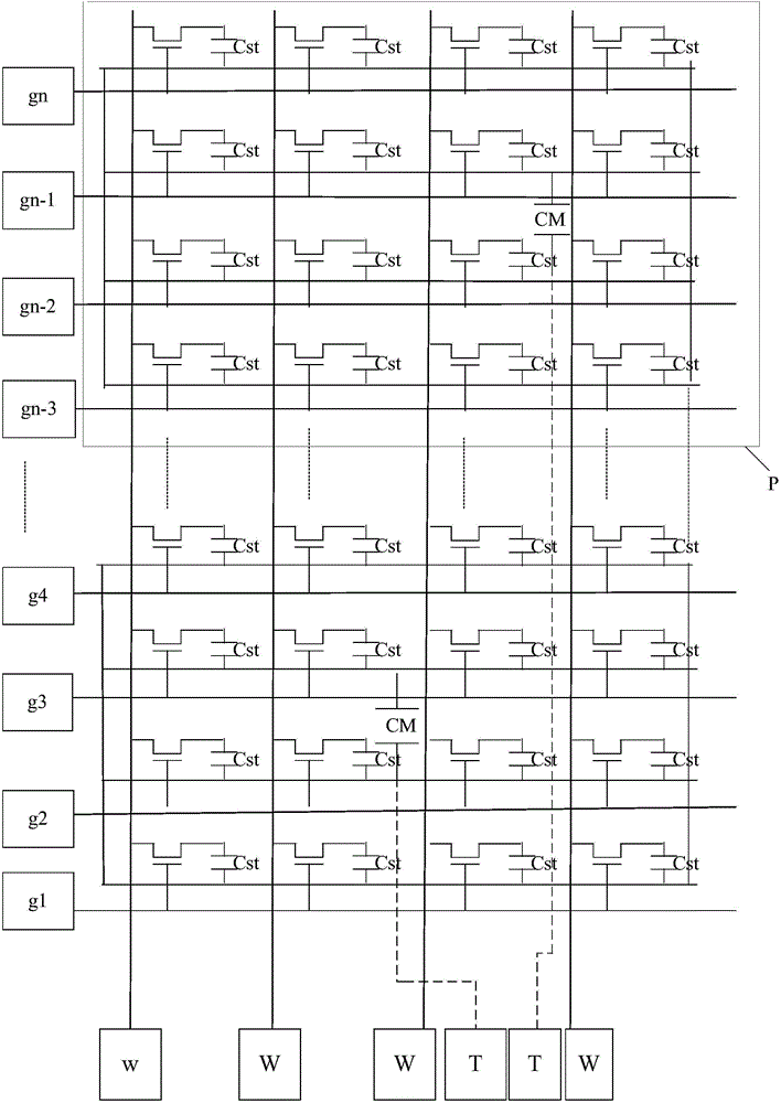
technical field [0001] The invention relates to the technical field of liquid crystal displays, in particular to an array substrate, a display panel and electronic equipment. Background technique [0002] see figure 1 , which is an equivalent circuit diagram of an array substrate with a touch function in the prior art. [0003] In the prior art, the common electrode layer is divided into multiple independent units, and each independent unit serves as a touch electrode P. [0004] figure 1 Except for the dotted line connected to the touch detection terminal T, the others are equivalent circuits of the liquid crystal display device. The area where each touch electrode P is located includes a plurality of thin film transistors (TFT, Thin Film Transistor). [0005] figure 1 The middle pulse signal g1-gn is connected as a scan line, such as figure 1 As shown, the scan line is connected to the gate of the TFT in each sub-pixel, and is used to control the switching state of t...
Claims
Application Information
Patent Timeline
Application Date:The date an application was filed.
Publication Date:The date a patent or application was officially published.
First Publication Date:The earliest publication date of a patent with the same application number.
Issue Date:Publication date of the patent grant document.
PCT Entry Date:The Entry date of PCT National Phase.
Estimated Expiry Date:The statutory expiry date of a patent right according to the Patent Law, and it is the longest term of protection that the patent right can achieve without the termination of the patent right due to other reasons(Term extension factor has been taken into account ).
Invalid Date:Actual expiry date is based on effective date or publication date of legal transaction data of invalid patent.

