Pixel circuit, driving method thereof, and display device
A technology for pixel circuits and drive transistors, applied in circuits, electrical components, and electric solid-state devices, can solve problems such as short light-emitting time and long programming time, and achieve the effects of simple structure, fewer control lines, and compensation for inhomogeneity
- Summary
- Abstract
- Description
- Claims
- Application Information
AI Technical Summary
Problems solved by technology
Method used
Image

Examples
Embodiment 1
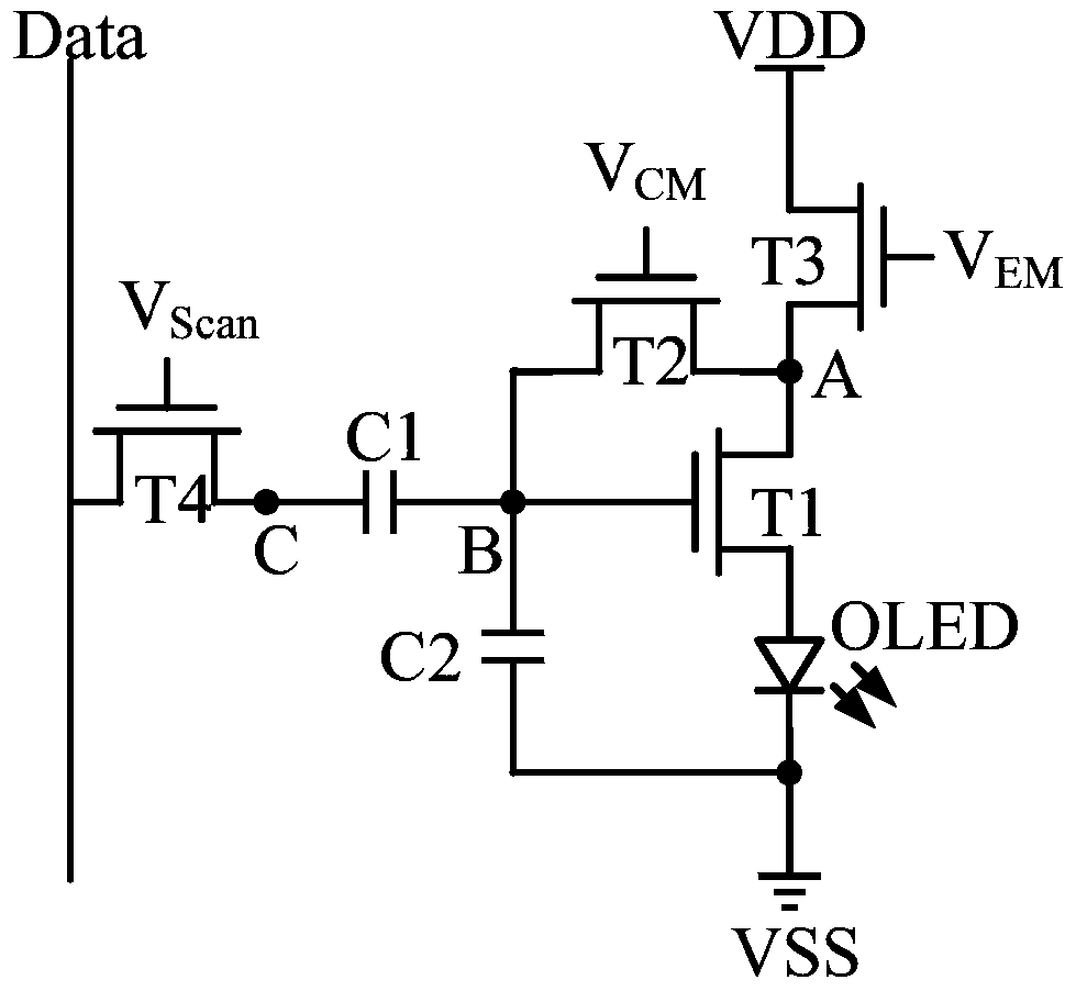
[0037] Please refer to Figure 3a with Figure 3b , which is a structural diagram of a pixel circuit disclosed in this embodiment, including: a driving transistor T1 and a light emitting element OLED connected in series between the first level terminal VDD and the second level terminal VSS, and the second transistor T2, the third The transistor T3, the fourth transistor T4, the first capacitor C1 and the second capacitor C2. in, Figure 3a In the pixel circuit shown, each transistor (driving transistor T1, second transistor T2, third transistor T3 and fourth transistor T4) is an N-type thin film transistor; Figure 3b In the pixel circuit shown, each transistor (driving transistor T1 , second transistor T2 , third transistor T3 and fourth transistor T4 ) is a P-type thin film transistor.
[0038] The first pole of the driving transistor T1 is connected to the second pole of the third transistor T3 to form the first node A; the second pole of the driving transistor T1 is con...
Embodiment 2
[0055] Please refer to Figure 5a with Figure 5b , is a structure diagram of a pixel circuit disclosed in this embodiment. The difference from the above-mentioned embodiments is that the pixel circuit disclosed in this embodiment further includes: a fifth transistor T5 providing a reference level V to the third node C ref transmitted by the fifth transistor T5.
[0056] The first pole of the fifth transistor T5 is used to input the reference level V ref , the second pole of the fifth transistor T5 is connected to the third node C, and the control pole of the fifth transistor T5 is used to input the first control signal V CM . In one example, please refer to Figure 5a , each transistor is an N-type transistor, the active level of each transistor is high level, the dark data voltage is low level, the initialization potential of the first node A and the second node B is provided by the first level terminal VDD; For another example, please refer to Figure 5b Each transist...
Embodiment 3
[0060] Please refer to Figure 6a with Figure 6b , is a schematic diagram of a pixel circuit structure disclosed in this embodiment. In the above embodiment, one end of the second capacitor C2 is directly connected to the control electrode of the driving transistor T1. In this embodiment, the second capacitor C2 is indirectly connected. connected to the control electrode of the drive transistor T1, and one end of the second capacitor C2 connected to the control electrode of the drive transistor T1 is connected to the third node C, through the coupling effect of the first capacitor C1, the end of the second capacitor C2 is connected to the drive transistor The control pole of T1 is electrically connected. In the pixel circuit disclosed in this embodiment, the connection manners of other components are the same as those in the above embodiments, and will not be repeated here.
[0061] Figure 6a In the pixel circuit shown, each transistor (driving transistor T1, second trans...
PUM
 Abstract
Description
Claims
Application Information
 - R&D
- Intellectual Property
- Life Sciences
- Materials
- Tech Scout
- Unparalleled Data Quality
- Higher Quality Content
- 60% Fewer Hallucinations
Browse by: Latest US Patents, China's latest patents, Technical Efficacy Thesaurus, Application Domain, Technology Topic, Popular Technical Reports.
© 2025 PatSnap. All rights reserved.Legal|Privacy policy|Modern Slavery Act Transparency Statement|Sitemap|About US| Contact US: help@patsnap.com