Display device, pixel circuit and driving method thereof

A technology of pixel circuits and driving transistors, applied in static indicators, instruments, etc., can solve the problems of non-compensation, uneven threshold voltage of TFT devices, uneven panel display, etc., and achieve the effect of compensating for unevenness

Active Publication Date: 2017-08-29
PEKING UNIV SHENZHEN GRADUATE SCHOOL
View PDF6 Cites 0 Cited by
  • Summary
  • Abstract
  • Description
  • Claims
  • Application Information

AI Technical Summary

Problems solved by technology

[0003] The pixel circuit of a traditional AMOLED is a simple two-thin film transistor (Thin Film Transistor, TFT) structure. Although this circuit has a simple structure, it cannot compensate the drift of the driving transistor T1 and OLED threshold voltage or because the TFT device is made of polycrystalline materials. As a result, the threshold voltage of the TFT devices across the panel is not uniform
When the threshold voltage of the driving transistor T1 and the OLED threshold voltage drift or the values ​​on the panel are inconsistent, the driving current I DS will change, and different pixels on the panel will drift differently due to different bias voltages, which will cause unevenness of the panel display

Method used


Image

  • Display device, pixel circuit and driving method thereof
  • Display device, pixel circuit and driving method thereof
  • Display device, pixel circuit and driving method thereof

Examples


Embodiment 1

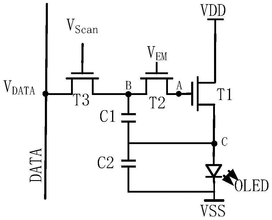
[0040] Please refer to Figure 1a with Figure 1b , The structure diagram of a pixel circuit disclosed in this embodiment includes: a driving transistor T1 and a light-emitting element OLED connected in series between a first level terminal VDD and a second level terminal VSS, and a second transistor T2, a third transistor Transistor T3 and storage capacitor C1. among them, Figure 1a In the pixel circuit shown, each transistor (the driving transistor T1, the second transistor T2, and the third transistor T3) is an N-type thin film transistor; Figure 1b In the pixel circuit shown, each transistor (the driving transistor T1, the second transistor T2, and the third transistor T3) is a P-type thin film transistor.

[0041] The first electrode of the driving transistor T1 is connected to the first terminal of the light emitting element OLED to form a third node C, and the second electrode of the driving transistor T1 and the second terminal of the light emitting element OLED are resp...

Embodiment 2

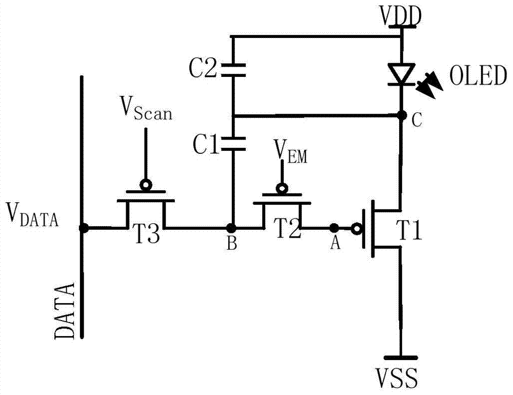
[0066] In the first embodiment, the initialization potential of the third node C is provided by the first level terminal VDD or the second level terminal VSS. The difference between this embodiment and the above embodiment is that the pixel circuit disclosed in this embodiment further includes a fourth The transistor T4 provides a corresponding potential to the third node C. Please refer to Figure 3a with Figure 3b , Is a structural diagram of a pixel circuit disclosed in this embodiment.

[0067] The first electrode of the fourth transistor T4 is connected to the third node C, the second electrode of the fourth transistor T4 is used to input the initialization potential, and the control electrode of the fourth transistor T4 is used to input the initialization control signal V Ini . In the initialization phase, the fourth transistor T4 responds to the initialization control signal V Ini The effective level of the fourth transistor T4 is turned on, and the second pole of the...

Embodiment 3

[0074] Please refer to Figure 6a with Figure 6b , The pixel circuit structure diagram disclosed in this embodiment is different from the above embodiment in that the second pole of the fourth transistor T4 is used for coupling to the data line DATA, and the initialization potential of the second pole of the fourth transistor T4 is set by the data line Provided by DATA.

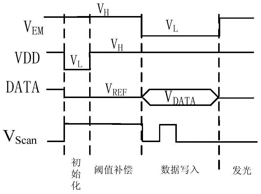
[0075] Please refer to Figure 7 , This example Figure 6a As shown in the driving timing diagram of the pixel circuit, the driving process of the pixel circuit of this embodiment is basically the same as that of the second embodiment. The difference is that in the initialization phase, the initialization potential of the third node C (for example, the low level V L ) Is provided by the data line DATA. In the threshold compensation stage and the data writing stage, the data line DATA provides the reference potential V to the third transistor T3 respectively REF And data voltage V DATA .

[0076] Figure 6a The s...


PUM


Abstract

A pixel circuit comprises: a driving transistor (T1) and a light emitting element serially-connected between a first power level end (VDD) and a second power level end (VSS), wherein a first gate of the driving transistor (T1) is connected to a first end of the light emitting element, a second transistor (T2) and a storage capacitor (C1) are connected between a control gate of the driving transistor (T1) and a conduction electrode. At an initialization stage, the second transistor (T2) conducts to separately initialize voltage levels of two ends of the storage capacitor (C1) and a voltage level of the control gate of the driving transistor (T1). At a threshold compensation stage, a reference voltage level (V REF) is provided to the control gate of the driving transistor (T1), so as to read a threshold voltage (V TH) of the driving transistor (T1) and store the same in the storage capacitor (C1), thereby compensating for the threshold voltage (V TH) of the driving transistor (T1) and inhomogeneity shown in the pixel circuit.

Description

Technical field [0001] This application relates to the field of display devices, and in particular to a display device and its pixel circuit and driving method. Background technique [0002] Organic Light-Emitting Diode (OLED) displays have been widely studied in recent years due to their advantages of high brightness, high luminous efficiency, wide viewing angle, and low power consumption, and have been rapidly applied to a new generation of displays. The driving mode of the OLED display can be passive matrix driving (Passive Matrix OLED, PMOLED) and active matrix driving (Active Matrix OLED, AMOLED). Although the cost of passive matrix driving is low, high-resolution display cannot be achieved due to the phenomenon of crosstalk, and the passive matrix driving current is large, which reduces the service life of the OLED. In contrast, the active matrix driving method sets a different number of transistors on each pixel as a current source, avoiding crosstalk, requiring less driv...

Claims


Application Information

Patent Timeline
Patent Type & Authority Patents(China)
IPC IPC(8): G09G3/3266G09G3/3233G09G3/325
CPCG09G2300/0819G09G3/32
Inventor 张盛东孟雪冷传利王翠翠
Owner PEKING UNIV SHENZHEN GRADUATE SCHOOL
Why Eureka
Try Eureka