Overlay error measuring device and method

A technology of overlay error and measuring device, which is applied in the field of integrated circuit manufacturing and can solve problems such as influence

Pending Publication Date: 2021-08-31
SHANGHAI MICRO ELECTRONICS EQUIP (GRP) CO LTD
View PDF8 Cites 1 Cited by
  • Summary
  • Abstract
  • Description
  • Claims
  • Application Information

AI Technical Summary

Problems solved by technology

[0005] The purpose of the present invention is to provide an overlay error measurement device and method to solve the influence of the unevenness of the measurement illumination spot itself on the overlay error measurement

Method used


Image

  • Overlay error measuring device and method
  • Overlay error measuring device and method
  • Overlay error measuring device and method

Examples


Embodiment Construction

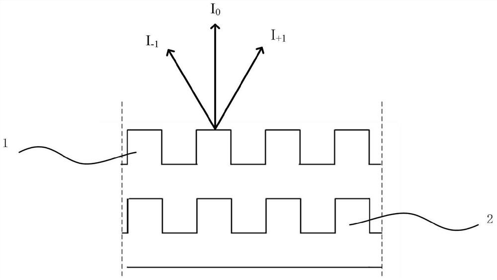
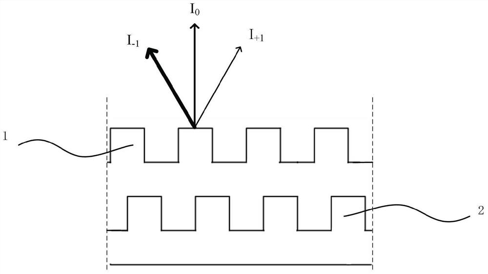
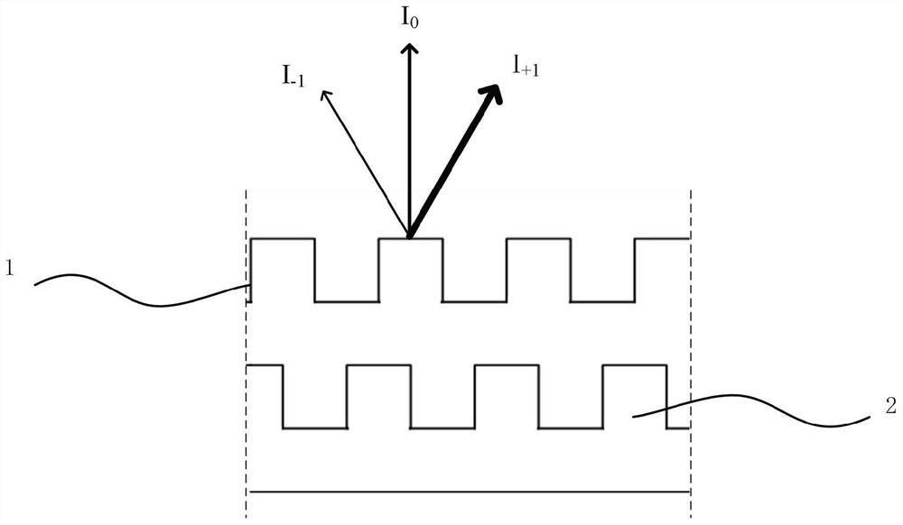
[0077] As mentioned above, in the commonly used devices or methods for measuring overlay errors, the influence of the non-uniformity of the measurement illumination spot itself on the overlay error is often ignored, or the calibration overlay mark is moved to make it located at the multi-point of the measurement illumination spot. The system is calibrated according to the sample measurement results at different positions, but due to too little sampled data, the characteristics of the marks used for calibration are not easy to control, and the calibration effect for the unevenness of the illumination spot itself is not good, and the calibration process is complex and time-consuming very long.

[0078] Therefore, there is a need for an overlay error measurement device and method that can achieve more accurate calibration of the non-uniformity of the measured illumination spot itself, thereby improving the detection performance of the photolithography machine and obtaining a more ...


PUM


Abstract

The invention provides an overlay error measuring device and method. The overlay error measuring device comprises an illumination unit, a light splitting device, an objective lens, a first detection unit and a data processor. The first detection unit comprises a first aperture diaphragm, and the first aperture diaphragm comprises at least one adjustable through hole. The through hole is adjusted, when the first aperture diaphragm is in a first state, the first detector obtains a first signal and transmits the first signal to the data processor, and when the first aperture diaphragm is in a second state, the first detector obtains a second signal and transmits the second signal to the data processor. The first signal is a calibration signal, the second signal is calibrated through the first signal, and the overlay error is calculated by using the calibrated second signal. Therefore, more accurate overlay errors can be obtained by using the overlay error measuring device and method, so that the detection performance of the overlay error measuring device is improved, and the working efficiency is improved.

Description

technical field [0001] The invention relates to the technical field of integrated circuit manufacturing, in particular to an overlay error measuring device and method. Background technique [0002] According to the lithography measurement technology roadmap given by the International Technology Roadmap for Semiconductors (ITRS), as the critical dimension (CD) of lithography patterns enters the process node of 22nm and below, especially double exposure (Double Patterning) and extreme ultraviolet lithography With the application and development of technology (EUVL), the measurement accuracy requirements for overlay of photolithography process parameters have entered the sub-nanometer field. Due to the limitation of imaging resolution limit, the traditional Imaging-Based overlay measurement technology based on imaging and image recognition (Imaging-Based overlay, IBO) has gradually been unable to meet the requirements of new process nodes for overlay measurement. Overlay measur...

Claims


Application Information

Patent Timeline
Patent Type & Authority Applications(China)
IPC IPC(8): G03F7/20
CPCG03F7/7085G03F7/70633
Inventor 杨晓青
Owner SHANGHAI MICRO ELECTRONICS EQUIP (GRP) CO LTD
Why Eureka
Try Eureka