Touch panel
A touch panel and touch area technology, applied in the fields of instruments, electrical digital data processing, data processing input/output process, etc. Wear and other problems to achieve the effect of reducing the area
- Summary
- Abstract
- Description
- Claims
- Application Information
AI Technical Summary
Problems solved by technology
Method used
Image
Examples
Embodiment Construction
[0031] The present invention will be further described in detail below in conjunction with the accompanying drawings and specific embodiments.
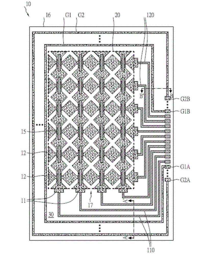
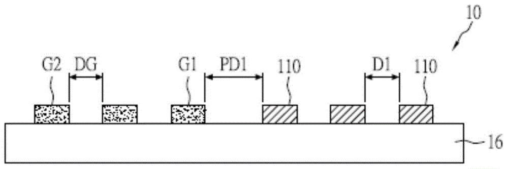
[0032] figure 1 Shown is a schematic diagram of a touch panel 10 according to an embodiment of the present disclosure. Please refer to figure 1 , The touch panel 10 includes a substrate 16 , a touch sensing electrode layer 17 , a plurality of signal wires 110 , 120 , and a plurality of ground wires G1 , G2 .
[0033] The substrate 16 is divided into a touch area 20 (shown as a dashed box) and a peripheral area 30 surrounding the touch area 20 . In one embodiment of the present invention, the material of the substrate 16 can be selected from glass, acrylic (PMMA), polyvinyl chloride (PVC), polypropylene (PP), polyethylene terephthalate (PET) , polyethylene naphthalate (PEN), polycarbonate (PC), polystyrene (PS) and other transparent materials.
[0034] The touch sensing electrode layer 17 is located in the touch area 20 and part of...
PUM
 Abstract
Description
Claims
Application Information


