Thick copper plate manufacturing method

A production method and technology of thick copper plate, applied in the direction of multi-layer circuit manufacturing, printed circuit manufacturing, electrical components, etc., can solve the problems of high failure rate, waste of resources, uneven unevenness, reduce waste of resources and improve white edge of lamination , the effect of improving the pass rate

Inactive Publication Date: 2015-11-18
SHENZHEN SUNTAK MULTILAYER PCB
View PDF6 Cites 6 Cited by
  • Summary
  • Abstract
  • Description
  • Claims
  • Application Information

AI Technical Summary

Problems solved by technology

[0004] For this reason, the technical problem to be solved by the present invention is to overcome technical bottlenecks such as white edges in the pressing process, lack of glue in the pressing process, uneven PCB, high failure rate and waste of resources, etc., thereby proposing a method with simple process and low cost Method for making thick copper plate with low cost and high pressing efficiency

Method used


Image

  • Thick copper plate manufacturing method
  • Thick copper plate manufacturing method

Examples


Embodiment

[0025] This embodiment discloses a method for manufacturing a thick copper plate, and the specific steps are as follows:

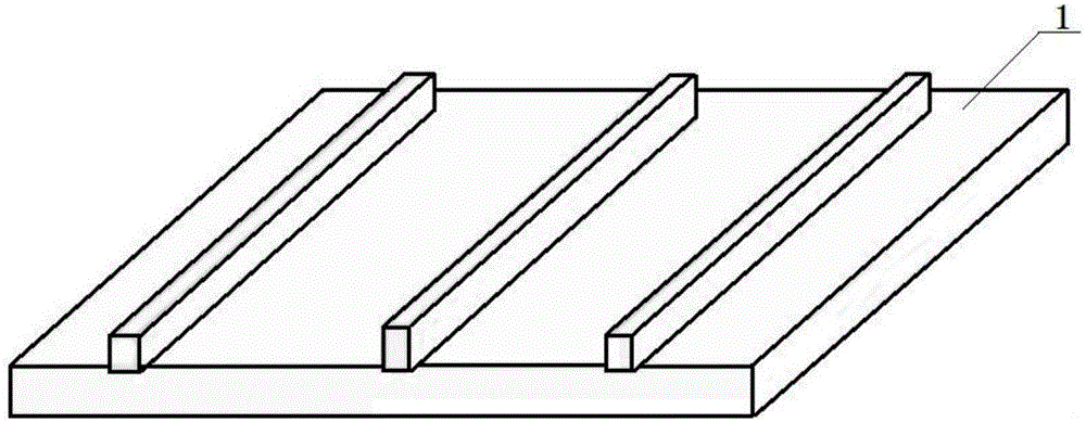
[0026] S1. Cutting process: Cut out the core board 1 according to the size of the jigsaw panel;

[0027] S2. Inner layer graphic processing: complete the inner layer circuit exposure with a 15-grid exposure ruler, and etch out the circuit graphics after development, such as figure 1 shown;

[0028] S3. Inner layer AOI processing: check the open and short circuit defects of the inner layer graphics and make corrections;

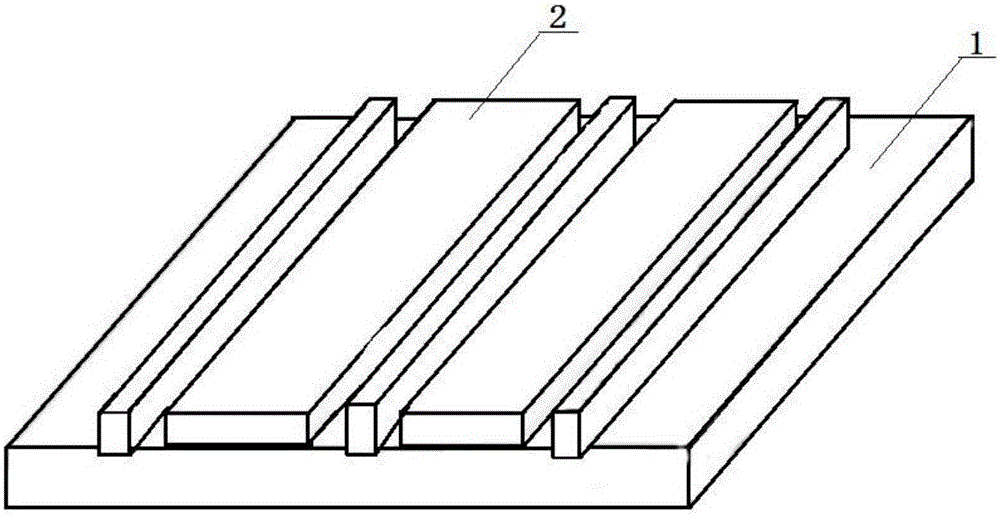
[0029] S4. Base material screen printing resin treatment: out of the stop point film, according to the solder mask screen printing out of the stop point net, block the position of the inner layer graphics, and fill the copper-free area with resin 2, such as figure 2 shown;

[0030] S5. Carry out the first baking board treatment: the temperature of the baking board is 155° C., and the duration is 1 hour, thereby curing the resin 2;

[...


PUM


Abstract

The invention belongs to the circuit board processing field, and more specifically relates to a thick copper plate manufacturing method. Through changing a resin glue filling flow, the method can well improve the problems of stitching white edges, stitching starvation and pcb unevenness in a stitching process, effectively improve a thick copper pcb, allow the internal layer copper thickness to be greater than 30 Z, and increase a qualified rate of stitching manufacture; accordingly, the method reduces resource waste, accords with the idea of energy conversation and environmental protection, reduces costs, and has a great prospect of use and large economic value.

Description

technical field [0001] The invention belongs to the field of circuit board processing, and in particular relates to a method for manufacturing a thick copper board. Background technique [0002] At present, the production of thick copper plates is made according to the normal process of lamination or with cushion pads. There have been problems such as white edges after lamination and poor glue addition. After normal pressing, because the inner layer copper is too thick (inner layer copper thickness > 30Z), the glue flow is insufficient during the pressing process, causing problems such as glue holes or white edges after pressing. The effect of extrusion can improve the poor lamination and glue addition, but after lamination, the board surface of the pcb is uneven after lamination. [0003] Therefore, it is the current circuit to provide a method for overcoming technical bottlenecks such as white edges during lamination, lack of glue during lamination, unevenness of PCB, ...

Claims


Application Information

Patent Timeline
Patent Type & Authority Applications(China)
IPC IPC(8): H05K3/46
CPCH05K3/4632H05K2203/068
Inventor 王佐周文涛朱拓王淑怡
Owner SHENZHEN SUNTAK MULTILAYER PCB
Why Eureka
Try Eureka