
Board-level fan-out chip packaging device and manufacturing method thereof

A chip packaging, fan-out technology, used in semiconductor/solid-state device manufacturing, semiconductor devices, electric solid-state devices, etc., can solve problems such as development and cost reduction, and achieve the effect of improving performance, eliminating dependencies, and improving heat dissipation performance.

Active Publication Date: 2019-04-26
广东佛智芯微电子技术研究有限公司
View PDF10 Cites 0 Cited by
  • Summary
  • Abstract
  • Description
  • Claims
  • Application Information

AI Technical Summary

Problems solved by technology

However, at present, many placement machines (DB equipment) cannot meet the needs of increasing board size and higher precision requirements, which limits the further development of this technology and the reduction of costs

Method used


Image

  • Board-level fan-out chip packaging device and manufacturing method thereof
  • Board-level fan-out chip packaging device and manufacturing method thereof
  • Board-level fan-out chip packaging device and manufacturing method thereof

Examples


preparation example Construction

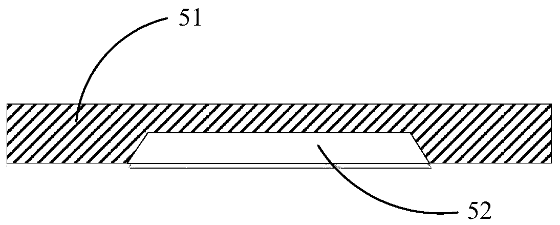
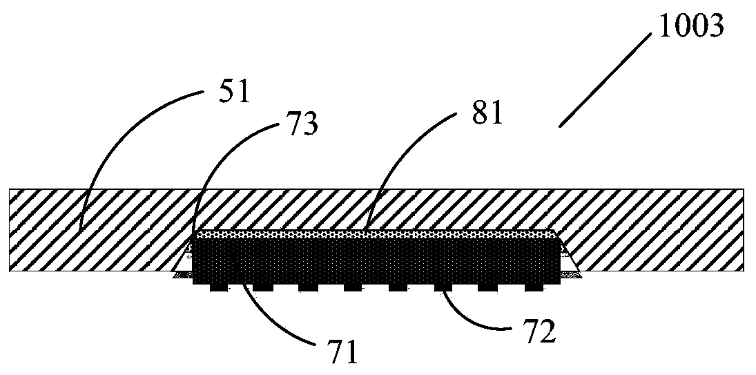
[0038] Therefore, the manufacturing method of the board-level fan-out type chip packaging device provided according to the embodiment of the present invention includes: providing a carrier board, on which a recess is provided, and the size of the recess is suitable for accommodating the chip; The back mount of the carrier board and the recess of the carrier board; the dielectric layer is arranged on the recessed side of the carrier board, on the carrier board and the chip; and by pressing the carrier board and the dielectric layer, the material of the dielectric layer can be filled to the in the gap between the recess of the carrier board and the chip.

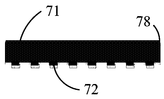
[0039] The structure of the chip packaging device 10 according to the embodiment of the present invention has been reflected in the introduction of the above process flow, for example Figure 3-Figure 9 Its cross-section is shown. Such as Figure 4 As shown, the board-level fan-out chip packaging device 1004 includes: a carr...


PUM


Abstract

The embodiment of the invention relates to a board-level fan-out chip packaging device and a preparation method thereof. A recess is formed in one side of a bearing board used for bearing a chip, the size of the recess is matched with the size of the back side of the chip, and the chip is mounted in the recess. When the chip is mounted to the bearing board, the recess in the bearing board exactly accommodates the back side of the chip, so that the chip to be packaged is easy and convenient to put in place. According to the invention, the dependence of fan-out packaging on the format of a chip mounter and chip mounting precision is eliminated, so that the development of the large-format fan-out chip packaging technology is facilitated.

Description

technical field [0001] The invention relates to the technical field of chip packaging, and more specifically, to a fan-out chip packaging device and a preparation method thereof. Background technique [0002] With the continuous development of information technology and semiconductor technology, electronic devices such as mobile phones, PADs, and smart watches are gradually showing a trend of light weight and integrated functions. This requires higher and higher integration of chips, which in turn brings unprecedented challenges to chip packaging. Increasing interconnect pitch mismatches, adding various chips with different functions, and reducing package size in the same footprint to increase battery size for longer life have opened windows for innovative embedded packaging technologies. [0003] Benefiting from the development of 3D Through-Silicon Via (TSV) technology, Fan-Out Wafer-Level Packaging (FOWLP) is currently considered to be the most suitable for the demanding...

Claims


Application Information

Patent Timeline
Patent Type & Authority Patents(China)
IPC IPC(8): H01L23/13H01L23/367H01L23/373H01L21/58H01L21/68
CPCH01L24/19H01L2224/04105H01L2224/12105H01L2224/19H01L2224/20H01L2224/32225H01L2224/32245H01L2224/73267H01L2224/92244H01L2924/15156H01L2924/00012
Inventor 郭学平
Owner 广东佛智芯微电子技术研究有限公司
Features
  • Generate Ideas
  • Intellectual Property
  • Life Sciences
  • Materials
  • Tech Scout
  • Unparalleled Data Quality
  • Higher Quality Content
  • 60% Fewer Hallucinations
Learn More