
Swing device and its adjustment method

An adjustment method and technology of silicon wafers, applied in photovoltaic power generation, electrical components, climate sustainability, etc., can solve problems such as complex methods and affecting the production efficiency of crystalline silicon solar cells, so as to improve production efficiency, fast chip placement, The effect of solving the patch problem

Active Publication Date: 2016-08-31
BEIJING NAURA MICROELECTRONICS EQUIP CO LTD
View PDF3 Cites 0 Cited by
  • Summary
  • Abstract
  • Description
  • Claims
  • Application Information

AI Technical Summary

Problems solved by technology

[0004] The embodiment of the present invention provides a device for swinging the film and its adjustment method, which solves the technical problem that the existing method for adjusting the film is relatively complicated and affects the production efficiency of crystalline silicon solar cells

Method used


Image

  • Swing device and its adjustment method
  • Swing device and its adjustment method
  • Swing device and its adjustment method

Examples


Embodiment Construction

[0032] The following will clearly and completely describe the technical solutions in the embodiments of the present invention with reference to the drawings in the embodiments of the present invention.

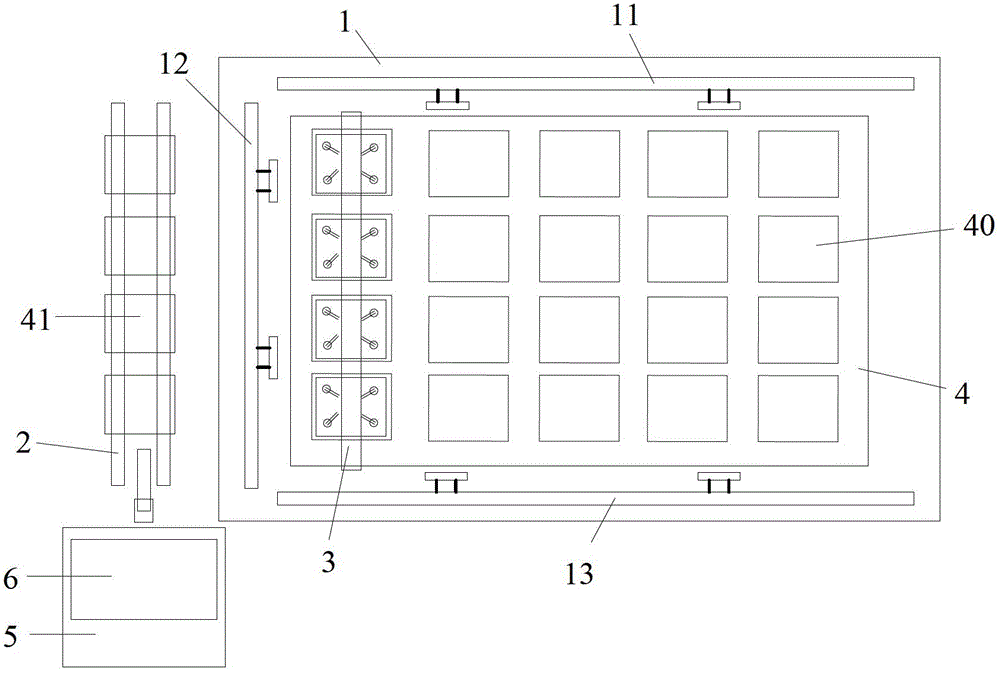
[0033] Such as figure 1 As shown, the film swing device provided by the embodiment of the present invention includes a loading platform 1 , a conveyor belt 2 and a gantry 3 . The loading platform 1 is used to carry the carrier plate 4, and the carrier plate 4 is provided with several slots 40 for placing silicon wafers 41; the loading platform 1 is provided with at least three positioners for adjusting from at least three directions And fix the position of the carrier board. As a preferred solution, the number of locators in this embodiment is three, and the first locator 11, the second locator 12, and the third locator 13 are respectively arranged on the front side, the left side and the left side of the loading platform 1. The rear side, that is, exerts pressure on the car...


PUM


Abstract

The embodiments of the invention belong to the technical field of semiconductor wafer processing, and disclose a wafer arranging apparatus and an adjusting method thereof, for solving the technical problem of affected production efficiency of crystalline silicon solar cells due to a quite complex method for adjusting a wafer overlapping problem. The water arranging apparatus comprises a loading bench, a conveyer belt and a portal frame. The loading bench is used for bearing a support plate, and the support plate is provided with a plurality of wafer grooves for arranging silicon wafers therein; the loading bench is provided with at least three positioning devices for adjusting and fixing the position of the support plate from at least three directions; the conveyer belt is disposed at one side of the loading bench for conveying the silicon wafers to be arranged; and the portal frame is used for arranging the silicon wafers on the conveyer belt on the support plate. The adjudging method comprises: when the silicon wafers are deviated from the wafer grooves, obtaining deviation distances of the silicon wafers; and according to the deviation distances of the silicon wafers, adjusting the positions of the support plate, the conveyer belt or the portal frame. The apparatus and the method provided by the invention are applied to a PECVD system for manufacturing the crystalline silicon solar cells.

Description

technical field [0001] The invention belongs to the technical field of semiconductor wafer processing, and in particular relates to a wafer swing device and an adjustment method thereof. Background technique [0002] With the continuous development of solar technology, crystalline silicon solar cells, as an emerging clean and renewable energy source, have been more and more widely used. The manufacture of crystalline silicon solar cells requires the use of a plasma enhanced chemical vapor deposition (Plasma Enhanced Chemical Vapor Deposition, PECVD) system. In the PECVD system, silicon wafers are first placed from the conveyor belt to the loading table by the gantry. In the carrier plate (layout process), it enters the preheating chamber, process chamber, cooling chamber, unloading table, etc. in the PECVD system for processing. The clamping cylinder set on the loading platform can fix the carrier on the loading platform, and there are several slots for placing silicon wafe...

Claims


Application Information

Patent Timeline
Patent Type & Authority Patents(China)
IPC IPC(8): H01L31/18H01L21/68
CPCH01L21/68H01L31/1876Y02E10/50Y02P70/50
Inventor 韩盼盼
Owner BEIJING NAURA MICROELECTRONICS EQUIP CO LTD
Features
  • Generate Ideas
  • Intellectual Property
  • Life Sciences
  • Materials
  • Tech Scout
  • Unparalleled Data Quality
  • Higher Quality Content
  • 60% Fewer Hallucinations
Learn More