
Board-level fan-out chip packaging device and manufacturing method thereof

A chip packaging and fan-out technology, which is applied in semiconductor/solid-state device manufacturing, electric solid-state devices, semiconductor devices, etc., can solve the problems of development and cost reduction, and achieve the effects of improving performance, improving heat dissipation performance, and eliminating dependencies

Active Publication Date: 2018-01-16
广东佛智芯微电子技术研究有限公司
View PDF6 Cites 0 Cited by
  • Summary
  • Abstract
  • Description
  • Claims
  • Application Information

AI Technical Summary

Problems solved by technology

However, at present, many placement machines (DB equipment) cannot meet the needs of increasing board size and higher precision requirements, which limits the further development of this technology and the reduction of costs

Method used


Image

  • Board-level fan-out chip packaging device and manufacturing method thereof
  • Board-level fan-out chip packaging device and manufacturing method thereof
  • Board-level fan-out chip packaging device and manufacturing method thereof

Examples


preparation example Construction

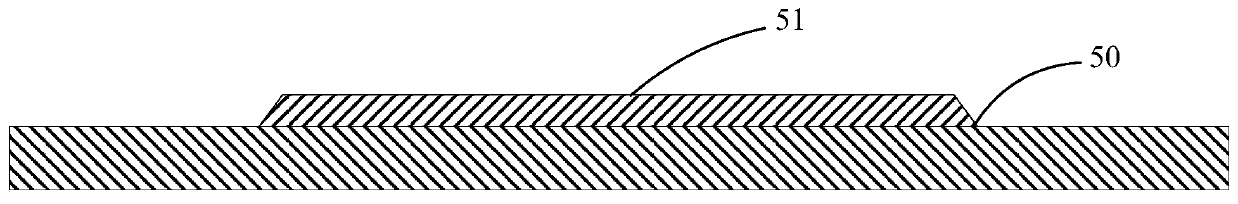
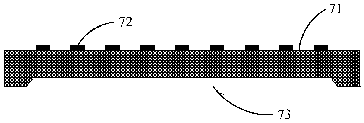
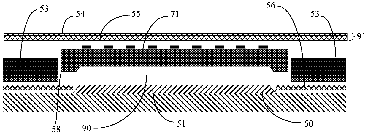
[0044] Therefore, the method for manufacturing a board-level fan-out chip packaging device provided according to an embodiment of the present invention includes: providing a carrier board on which bumps are provided; arranging a first dielectric around the bumps on the carrier board layer; arranging a core board on the dielectric layer, wherein the core board is provided with an opening, and the opening of the core board surrounds the bump; embedding the chip in the opening of the core board, wherein the backside of the chip has a size matching the bump The recess of the chip is embedded so that the recess of the back of the chip is engaged with the bump of the carrier board, and the core board surrounds the chip; a second dielectric layer is arranged on the embedded structure of the chip and the core board; and by extruding the chip and The embedding structure of the core board, the carrier board and the dielectric layer enables the material of the dielectric layer to fill the...


PUM


Abstract

The invention relates to a board-level fan-out chip packaging device and a preparation method therefor. A recess is arranged in the back surface of the chip. A projection matching the recess in size is arranged on a loading plate of a packaging chip, and therefore it is easy and convenient to keep a chip to be packaged to take its place. Through the packaging device, fan-out packaging is independent from a breadth of a chip mounter and chip mounting precision, and thus development of a fan-out chip packaging technology with a large breadth is possible.

Description

technical field [0001] The invention relates to the technical field of chip packaging, and more specifically, to a fan-out chip packaging device and a preparation method thereof. Background technique [0002] With the continuous development of information technology and semiconductor technology, electronic devices such as mobile phones, PADs, and smart watches are gradually showing a trend of light weight and integrated functions. This requires higher and higher integration of chips, which in turn brings unprecedented challenges to chip packaging. Increasing interconnect pitch mismatches, adding various chips with different functions, and reducing package size in the same footprint to increase battery size for longer life have opened windows for innovative embedded packaging technologies. [0003] Benefiting from the development of 3D Through-Silicon Via (TSV) technology, Fan-Out Wafer-Level Packaging (FOWLP) is currently considered to be the most suitable for the demanding...

Claims


Application Information

Patent Timeline
Patent Type & Authority Patents(China)
IPC IPC(8): H01L23/31H01L23/367H01L21/56
CPCH01L24/19H01L2224/04105H01L2224/12105H01L2224/19H01L2224/32245H01L2224/73267H01L2924/15159H01L2924/18162H01L2924/00012
Inventor 郭学平
Owner 广东佛智芯微电子技术研究有限公司
Features
  • Generate Ideas
  • Intellectual Property
  • Life Sciences
  • Materials
  • Tech Scout
  • Unparalleled Data Quality
  • Higher Quality Content
  • 60% Fewer Hallucinations
Learn More