
Chip gland jig and process method thereof

A technology of chips and fixtures, which is applied in the direction of electrical components, semiconductor/solid-state device manufacturing, circuits, etc., can solve the problems of lower product yield, inconsistent total height of chips and glue, and inability to accurately control the paste height, so as to improve the placement quality effect

Pending Publication Date: 2020-07-14
星科金朋半导体(江阴)有限公司
View PDF0 Cites 0 Cited by
  • Summary
  • Abstract
  • Description
  • Claims
  • Application Information

AI Technical Summary

Problems solved by technology

Uncertain factors such as the consistency and temperature of the glue will affect the total height of the chip and the glue, resulting in inconsistent total heights of the chip and the glue, and the pasting height cannot be precisely controlled. Especially for some unconventional chips, the surface texture is irregular, and the machine cannot Judgment, reducing the yield of the product

Method used


Image

  • Chip gland jig and process method thereof
  • Chip gland jig and process method thereof
  • Chip gland jig and process method thereof

Examples


Embodiment Construction

[0056] Specific embodiments of the present invention will be described in detail below in conjunction with the accompanying drawings. For ease of description, spatially relative terms (such as "below," "beneath," "lower," "above," "upper," etc.) may be used to describe the relationship between one element or component and another shown in the figures. Component or part relationship. Spatially relative terms encompass different orientations of the device in use or operation in addition to the orientation depicted in the figures. The device may be otherwise oriented (rotated 90 degrees or at other orientations) and the spatially relative descriptions used herein should be interpreted similarly accordingly.

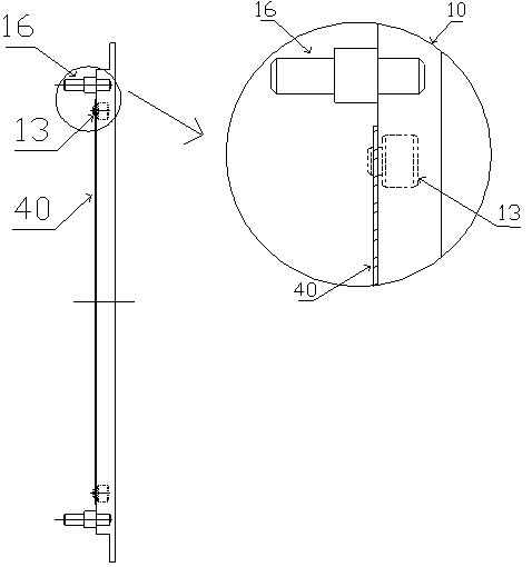
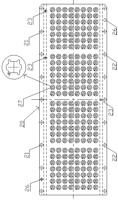
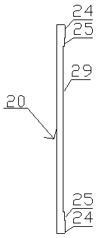
[0057] A chip capping jig of the present invention comprises a carrier 10, a stencil plate 20 and a stencil plate 30 from bottom to top, and a substrate 40 is placed between the carrier 10 and the stencil plate 20, as Figure 8 shown. Generally, one carrier 10 corresponds...


PUM


Abstract

The invention discloses a chip gland jig and a technological method thereof and belongs to the technical field of semiconductor jigs. The chip gland jig sequentially comprises a carrier (10), a character leaking plate (20) and a character pressing plate (30) from bottom to top; a base plate (40) is arranged between the carrier (10) and the word leaking plate (20); the chip mounting area of the base plate (40) faces upwards; a plurality of carrier fixing pieces I (11), a plurality of carrier fixing pieces II (12), a plurality of guide pins (13), a plurality of positioning long needles (16) anda plurality of vacuum hole arrays (18) are arranged on the carrier (10); the character leaking plate (20) is provided with a plurality of character leaking plate fixing pieces I (21), a plurality of character leaking plate fixing pieces II (22), a plurality of positioning holes (26), a plurality of blind holes (23) and a character leaking hole array; the character pressing plate (30) is provided with a plurality of character pressing plate fixing pieces I (31), a plurality of character pressing plate fixing pieces II (32), a plurality of positioning holes (36) and a protruding block array. With the chip gland jig and the technological method adopted, the consistency chip bonding height can be controlled.

Description

technical field [0001] The invention relates to a chip capping jig and a process method thereof, belonging to the technical field of semiconductor jigs. Background technique [0002] In the semiconductor integrated circuit manufacturing process, it is necessary to paste the chip to the patch on the substrate or lead frame, and it is necessary to control the total height of the chip and the glue. Uncertain factors such as the consistency and temperature of the glue will affect the total height of the chip and the glue, resulting in inconsistent total heights of the chip and the glue, and the pasting height cannot be precisely controlled. Especially for some unconventional chips, the surface texture is irregular, and the machine cannot Judgment reduces the yield rate of the product. Contents of the invention [0003] The object of the present invention is to overcome the deficiencies in the prior art, and provide a chip capping jig capable of controlling the bonding height ...

Claims


Application Information

Patent Timeline
Patent Type & Authority Applications(China)
IPC IPC(8): H01L21/67H01L21/50H01L21/56
CPCH01L21/50H01L21/56H01L21/67144
Inventor 徐堃丹尼罗沈国强薛文华
Owner 星科金朋半导体(江阴)有限公司
Features
  • Generate Ideas
  • Intellectual Property
  • Life Sciences
  • Materials
  • Tech Scout
  • Unparalleled Data Quality
  • Higher Quality Content
  • 60% Fewer Hallucinations
Learn More