Transistor based charge control guide circuit of electric vehicle

A technology of electric vehicles and guiding circuits, which is applied to electric vehicles, battery circuit devices, circuit devices, etc., can solve problems such as unfavorable costs and complex guiding circuits, and achieve cost saving, low price, and peak voltage maintenance.

Inactive Publication Date: 2015-12-16
QINGDAO UNIV +1
5 Cites 3 Cited by

AI-Extracted Technical Summary

Problems solved by technology

In the prior art, the electric vehicle charging control pilot circu...

Abstract

The invention discloses a transistor based charge control guide circuit of an electric vehicle conforming to national standards, and belongs to the field of electric vehicles. The transistor based charge control guide circuit comprises a power supply connection detecting module, a level conversion module and a level detecting module; a connection state between a power supply plug and a power supply socket is judged according to the output voltage of the power supply connection detecting module; the level conversion module takes the transistor as the main device for receiving PWM signals output by a power supply control apparatus and converting the PWM signals into plus or minus 12V PWM signals according to national standards; and the level detecting module maintains the voltage peak value output by the level conversion module to enable the power supply control apparatus to collect the voltage peak value so as to judge a connection state of a charging interface and a state of a vehicle control apparatus based on the voltage peak value, when conditions are met, the power supply control apparatus charges the electric vehicle. The level detecting module of the transistor based charge control guide circuit has the functions of maintaining the voltage pack value and improving the load drive capacity; and in addition, the devices adopted by the transistor based charge control guide circuit are low in cost, so that the transistor based charge control guide circuit is low in costs and has promotional value.

Application Domain

Batteries circuit arrangementsElectric power

Technology Topic

Peak valueElectric vehicle +7

Image

  • Transistor based charge control guide circuit of electric vehicle

Examples

  • Experimental program(1)

Example Embodiment

[0019] The present invention will be further described in detail below in conjunction with the drawings and specific implementations:
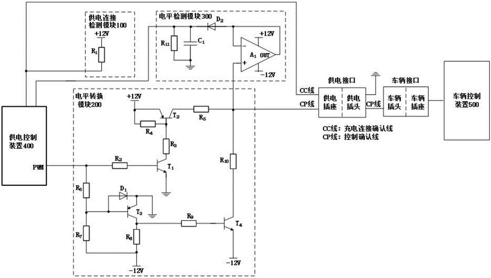
[0020] Such as figure 1 As shown, a transistor-based electric vehicle charging control steering circuit includes: a power supply connection detection module 100, a level conversion module 200, and a level detection module 300; wherein:
[0021] The power supply connection detection module 100 is used to output voltage to the power supply control device 400. The power supply connection detection module 100 includes a first resistor R1. One end of the first resistor R1 is connected to a +12V first power supply voltage, and the other end is connected to a power supply socket Connect through the CC (charging connection confirmation) line. When the power supply plug is connected to the power supply socket, the output voltage of the power supply connection detection module 100 is 0V; when the power supply plug is not connected to the power supply socket, the output voltage of the power supply connection detection module 100 is +12V. When the output voltage of the power supply connection detection module 100 is 0V, it is determined that the power supply plug is connected to the power supply socket, and the power supply control device 400 can send a pulse width modulation signal to output to the level conversion module 200.
[0022] The level conversion module 200 includes nine resistors including a second resistor, a third resistor, a fourth resistor, a fifth resistor, a sixth resistor, a seventh resistor, an eighth resistor, a ninth resistor, and a tenth resistor. The crystal triode, the second crystal triode, the third crystal triode, and the fourth crystal triode also include the first crystal diode. The second resistor R2 and the third resistor R3 are respectively connected to the base and collector of the first transistor T1, the other end of the second resistor R2 is connected to the pulse width modulation signal sent by the power supply control device 400, and the third The other end of the resistor R3 is connected to the base of the second transistor T2. The fourth resistor R4 is connected across the base and emitter of the second transistor T2, and one end of the fourth resistor R4 and the common end of the emitter of the second transistor T2 are connected to the first power supply voltage. One end of the fifth resistor R5 is connected to the collector of the second transistor T2, and the other end is connected to the level detection module, and is output to the vehicle control device 500 through the CP (control confirmation) line.
[0023] One end of the sixth resistor R6 and one end of the second resistor R2 form a common end connected to the port through which the power supply control device 400 sends a pulse width modulation signal, and the other end of the sixth resistor R6 and one end of the seventh resistor R7 form a common end connection To the base of the third transistor T3, the common end formed by the other end of the seventh resistor R7 and one end of the eighth resistor R8 is grounded; the other end of the eighth resistor R8 and one end of the ninth resistor R9 are formed The common terminal is connected to the collector of the third transistor T3, the other end of the ninth resistor R9 is connected to the base of the fourth transistor T4; one end of the tenth resistor R10 is connected to the fourth transistor T4 The common terminal composed of the other end of the tenth resistor R10 and the other end of the fifth resistor R5 is connected to the level detection module 300, and is connected to the vehicle control device 400 through the CP (control confirmation) line; the first The crystal diode D1 is connected across the base and the emitter of the third transistor T3, and the common terminal formed by the cathode of the first crystal diode D1 and the emitter of the third transistor T3 is grounded. The emitters of the first transistor and the fourth transistor T4 are grounded.
[0024] When the digital PWM wave is at a high level, the transmitting junctions of the first transistor T1 and the second transistor T2 are saturated and turned on by the forward voltage, and output a +12V high level. At this time, the third transistor and the fourth transistor are cut off . When the digital PWM wave is at a low level, the transmitting junctions of the third transistor T3 and the fourth transistor are saturated and turned on by the forward voltage, and output a high level of -12V. At this time, the first transistor and the second transistor T2 Deadline. Therefore, a reliable PWM wave signal with an amplitude of ±12V is obtained on the output CP (control confirmation) line of the level conversion module 200, and the level conversion module 200 outputs the PWM wave signal with an amplitude of ±12V to the vehicle control device.
[0025] The level detection module 300 includes a first integrated operational amplifier A1, a second crystal diode D2, an eleventh resistor R11 and a first capacitor C1. The same direction input terminal (+) of the first integrated operational amplifier A1 is connected to the common terminal composed of the fifth resistor R5 and the tenth resistor R10, and the reverse input terminal (-) of the first integrated operational amplifier A1 and its output terminal ( OUT) is connected to and connected to the anode of the second crystal diode D2, and the cathode of the second crystal diode D2 is connected to a common terminal formed by one end of the eleventh resistor R11 and one end of the first capacitor C1 and serves as an output terminal; The eleventh resistor R11 and the first capacitor C1 are connected in parallel, and the common end formed by the other end of the eleventh resistor R11 and the other end of the first capacitor C1 is connected to the ground.
[0026] The level detection module 300 is used to detect the output voltage of the level conversion module 200. The level detection module 300 maintains the peak value of this voltage and outputs the peak value of the voltage to the power supply control device 400, which is based on The voltage peak at this point can determine the connection state of the charging interface (power supply interface and vehicle interface) of the electric vehicle and the state of the vehicle control device 500. When the power supply interface is fully connected to the vehicle interface and the vehicle control device 500 allows charging, turn on the switch The power supply control device 400 supplies power to the electric vehicle. The main function of the level detection module 300 is to maintain the voltage peak value to achieve the purpose of maintaining the voltage peak value and enabling the power supply control device 400 to successfully collect the voltage peak value. Another function of the level detection module 300 is to improve the load driving capability.
[0027] The inverting input terminal of the first integrated operational amplifier A1 is connected to its output terminal to form a same direction follower; the output signal of the first integrated operational amplifier A1 is the same as the input signal of the same direction input terminal, and the function of the first integrated operational amplifier is Signal isolation and improve load driving capability. The first integrated operational amplifier A1 is connected to a unidirectional second crystal diode D2 and a resistor-capacitor parallel circuit (a circuit composed of the eleventh resistor R11 and the first capacitor C1 in parallel) to form a voltage peak holding circuit. When the resistance of the eleventh resistor R11 is 10k and the first capacitor C1 is 1μF, the discharge time constant is 10ms, which can ensure that the digital device with a sampling time of less than 1ms collects the peak voltage, thus meeting the voltage peak holding requirement.
[0028] In this embodiment, the first resistor R1 is 10k, the second resistor R2 is 47k, the third resistor R3 is 10k, the fourth resistor R4 is 47k, the fifth resistor R5 is 1k, the sixth resistor R6 is 100k, and the seventh resistor R7 is Take 100k, the eighth resistor R8 is 100k, the ninth resistor R9 is 47k, the tenth resistor R10 is 1k, and the eleventh resistor R11 is 10K. The first capacitor C1 is 1μF. The first integrated operational amplifier A1 uses LM258. The first crystal diode and the second crystal diode D2 both use 1N4148.
[0029] The charging control guide circuit of the invention can output a reliable PWM signal with an amplitude of ±12V. The circuit of the invention complies with the national standard of the AC charging interface of the connection device for conductive charging of electric vehicles. The level detection module of the invention has a peak voltage And the effect of improving the load driving ability, and the device adopted by the present invention is low in price, saves cost, and has good promotion value.
[0030] Of course, the above description is not a limitation of the present invention, and the present invention is not limited to the above examples. Changes, modifications, additions or substitutions made by those skilled in the art within the essential scope of the present invention shall also belong to the present invention. The scope of protection of the invention.

PUM

no PUM

Description & Claims & Application Information

We can also present the details of the Description, Claims and Application information to help users get a comprehensive understanding of the technical details of the patent, such as background art, summary of invention, brief description of drawings, description of embodiments, and other original content. On the other hand, users can also determine the specific scope of protection of the technology through the list of claims; as well as understand the changes in the life cycle of the technology with the presentation of the patent timeline. Login to view more.

Similar technology patents

Shank installation structure and cutters

InactiveUS6966730B1easy to worklow price
Owner:MIYANAGA KK
Why Eureka
Try Eureka