Supercharge Your Innovation With Domain-Expert AI Agents!

Circuit switched to chip testing mode by utilizing negative voltage

A chip testing, negative voltage technology, applied in the direction of logic circuits, electrical components, pulse technology, etc., can solve the problems of increasing chip cost and design complexity

Inactive Publication Date: 2015-12-30
XINBAI MICROELECTRONICS BEIJING
View PDF4 Cites 9 Cited by
  • Summary
  • Abstract
  • Description
  • Claims
  • Application Information

AI Technical Summary

Problems solved by technology

The above method involves non-volatile storage modules such as OTP, MTP and flash, which will increase the chip cost and design complexity

Method used


Image

  • Circuit switched to chip testing mode by utilizing negative voltage

Examples


Embodiment Construction

[0017] The following will clearly and completely describe the technical solutions in the embodiments of the present invention with reference to the accompanying drawings in the embodiments of the present invention. Obviously, the described embodiments are only some, not all, embodiments of the present invention. Based on the embodiments of the present invention, all other embodiments obtained by persons of ordinary skill in the art without making creative efforts belong to the protection scope of the present invention.

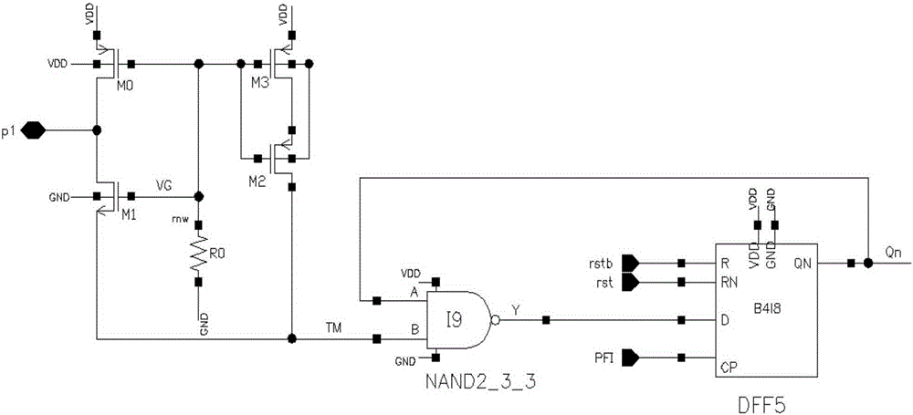
[0018] see figure 1 , a circuit that uses a negative voltage to enter a chip test mode, including a switch M0, a switch M1, a resistor R0, and an invertor I9, the source of the switch M0 is connected to the power supply VDD, and the drain of the switch M0 is connected to the chip tube The pin P1 and the drain of the switch tube M1, the gate of the switch tube M0 are connected to the resistor R0, the gate of the switch tube M1, the gate of the switch tube M2 an...


PUM


Abstract

The invention discloses a circuit switched to a chip testing mode by utilizing negative voltage. A source electrode of a switch tube M0 is connected with a power supply VDD, a drain electrode of the switch tube M0 is connected with a chip pin P1 and a drain electrode of a switch tube M1, a grid electrode of the switch tube M0 is connected with a resistor RO, a grid electrode of the switch tube M1, a grid electrode of a switch tube M2 and a grid electrode of a switch tube M3, the other end of the resistor RO is grounded, a source electrode of the switch tube M3 is connected with the power supply VDD, a source electrode of the switch tube M1 is connected with a source electrode of the switch tube M2 and the input end B of a NOT gate I9, the input end A of the NOT gate I9 is connected with an ON pin of a trigger DFF5, and a CP pin of the trigger DFF5 is connected with a chip pin PFI. The circuit can be switched to the chip testing mode by reusing an I / O pin and being matched with the exerted negative voltage, can still have multiple state modes under the condition that a process is not provided with a nonvolatile memory after chip package and does not influence normal application of a client.

Description

technical field [0001] The invention belongs to the field of integrated circuit design, and proposes a circuit that reuses I / O pins and needs to cooperate with the application of negative voltage to enter a test mode, simplifies the production test process, and facilitates analysis and debugging when a problem occurs in the chip. Background technique [0002] Various failures may occur in the semiconductor process: material defects and process deviations may cause problems such as short circuits, open circuits, and device-junction punch-through in the chip. Such physical failures will inevitably lead to failures in circuit function or performance. [0003] Through effective testing methods, it is used to locate faults in the manufacturing process and ensure the correctness of basic components such as wiring and transistors. The original design needs to be modified to include test logic that is only used during testing. Test logic not only facilitates the automatic generati...

Claims


Application Information

Patent Timeline
IPC IPC(8): H03K19/00
Inventor 阮为
Owner XINBAI MICROELECTRONICS BEIJING
Features
  • R&D
  • Intellectual Property
  • Life Sciences
  • Materials
  • Tech Scout
  • Unparalleled Data Quality
  • Higher Quality Content
  • 60% Fewer Hallucinations
Learn More