Manufacturing method of target assembly

A production method and target technology, which are applied in the production field of target components, can solve the problems of lack of binding performance, inability to obtain binding rate and binding strength of target components, etc.

CN105296943AInactive Publication Date: 2016-02-03KONFOONG MATERIALS INTERNATIONAL CO LTD
8 Cites 6 Cited by

Patent Information

Authority / Receiving Office
CN · China
Patent Type
Applications(China)
Current Assignee / Owner
Publication Date
2016-02-03
Estimated Expiration
Not applicable · inactive patent

Smart Images

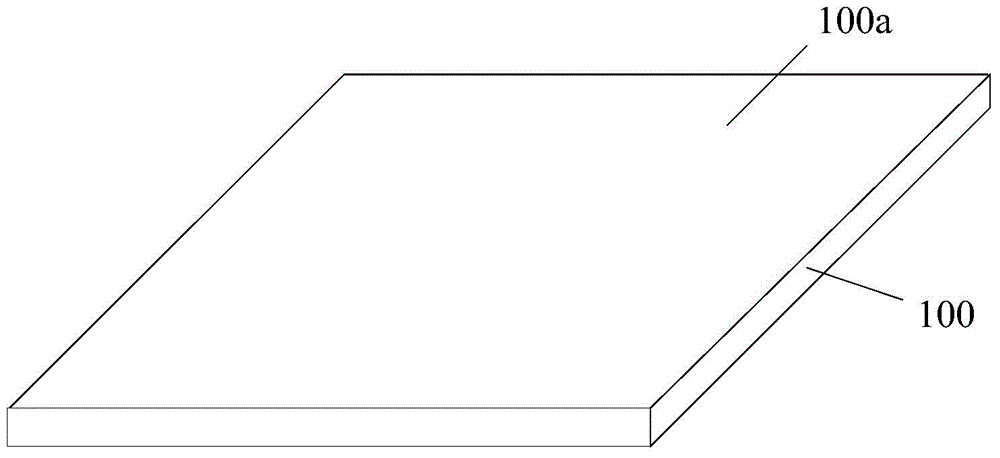
  • Figure 1
    Figure 1
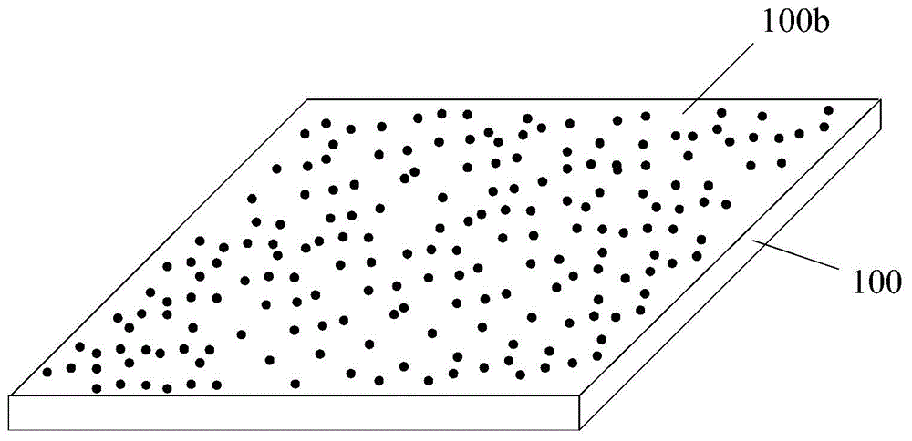
  • Figure 2
    Figure 2
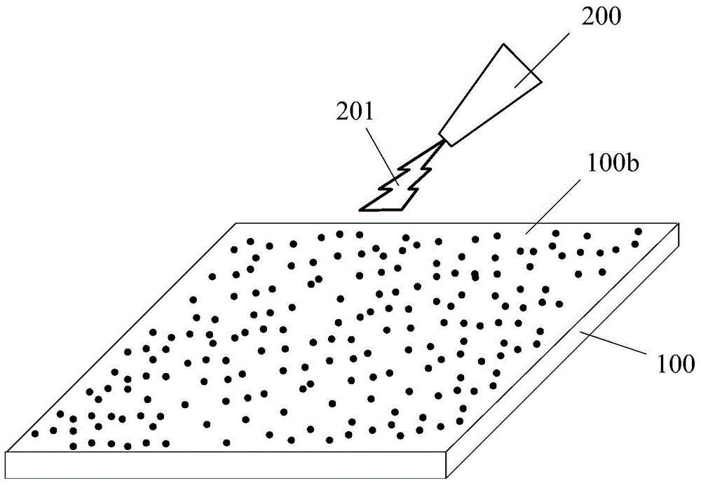
  • Figure 3
    Figure 3
Patent Text Reader

Abstract

The invention discloses a manufacturing method of a target assembly. The manufacturing method comprises the steps that a target made of molybdenum silicon material is provided; a to-be-welded surface of the target is subjected to sand blasting; the target is subjected to washing treatment after the sand blasting; the to-be-welded surface of the target is subjected to activating treatment after the washing treatment; a metal coating layer is formed on the to-be-welded surface of the target by adopting a chemical plating technology after the activating treatment; and the target is welded to a back plate by utilizing the metal coating layer. With the adoption of the manufacturing method of the target assembly, the target assembly formed by the molybdenum silicon material has sufficient binding rate and bonding strength.
Need to check novelty before this filing date? Find Prior Art

Description

technical field

[0001] The invention relates to the field of semiconductor manufacturing, in particular to a method for manufacturing a target assembly. Background technique

[0002] Generally, the target assembly is composed of a target and a backing plate that meet the sputtering performance. The backing plate may function as a support in the assembly of the target assembly to the sputtering stage and may conduct heat.

[0003] During the sputtering process, the working environment of the target assembly is relatively harsh, for example, the working temperature of the target assembly is relatively high. Moreover, one side of the target assembly is subjected to strong cooling with cooling water, while the other side is in a high vacuum environment of 10-9Pa, thereby forming a huge pressure difference on the opposite sides of the target assembly; furthermore, the target assembly In the high-voltage electric field and magnetic field, it will be bombarded by various particle...

Examples

Embodiment Construction

[0032] As mentioned in the background art, using the existing welding method, the direct welding of the molybdenum-silicon material and the back plate has a low bonding strength, which cannot meet the requirements of the semiconductor target, that is, the molybdenum-silicon material with the required bonding rate and bonding strength cannot be obtained. Target assembly.

[0033] To this end, the present invention provides a new method for forming a target assembly. The method first provides a molybdenum-silicon material target, and then performs sandblasting on the to-be-welded surface of the target. Then, the target material is rinsed, and after the rinse treatment is performed on the target material, an activation treatment is performed on the to-be-welded surface of the target material, and after the activation treatment, an electroless plating process is used to A metal plating layer is formed on the to-be-welded surface of the target material, and the target material and ...