SRAM memory cell, storage array and memory

A storage unit and storage array technology, applied in the field of storage arrays, memories, and SRAM storage units, can solve problems such as SRAM storage unit write operation failure, and achieve good write efficiency, simple circuit structure, and easy production and implementation.

Active Publication Date: 2016-02-17
SPREADTRUM COMM (SHANGHAI) CO LTD
View PDF5 Cites 2 Cited by
  • Summary
  • Abstract
  • Description
  • Claims
  • Application Information

AI Technical Summary

Problems solved by technology

[0025] The technical problem solved by the present invention is to provide a SRAM storage unit to solve the problem of write operation failure that may exist in the SRAM storage unit

Method used


Image

  • SRAM memory cell, storage array and memory
  • SRAM memory cell, storage array and memory
  • SRAM memory cell, storage array and memory

Examples


Embodiment Construction

[0061] In order to make the purpose, features and effects of the present invention more obvious and understandable, the specific implementation manners of the present invention will be described in detail below in conjunction with the accompanying drawings.

[0062] Many specific details are set forth in the following description to facilitate a full understanding of the present invention, but the present invention can also be implemented in other ways than described here, so the present invention is not limited by the specific embodiments disclosed below.

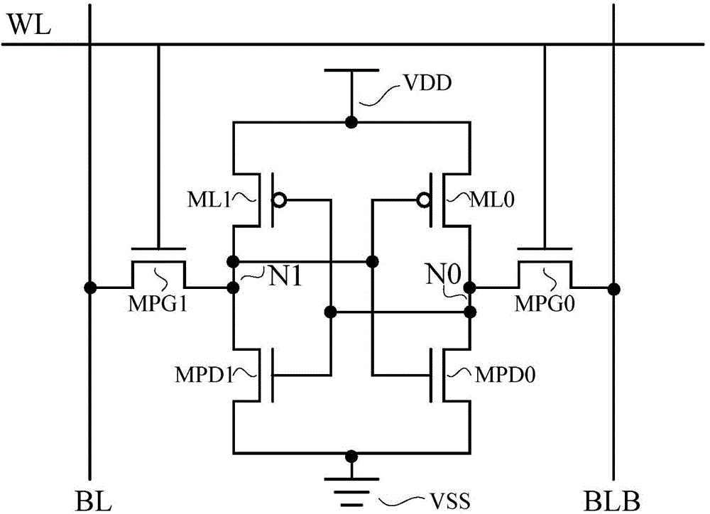
[0063] Such as Figure 4 The shown SRAM storage unit includes: a first PMOS transistor ML0, a second PMOS transistor ML1, a first NMOS transistor MPD0, a second NMOS transistor MPD1, a first pass transistor MPG0, a second pass transistor MPG1, a first double-gate The PMOS transistor MDP0 and the second double-gate PMOS transistor MDP1, the first pass transistor MPG0 and the second pass transistor MPG1 are all NMOS transist...


PUM


Abstract

The invention relates to a SRAM memory cell, a storage array and a memory. The SRAM memory cell comprises a first PMOS transistor, a second PMOS transistor, a first NMOS transistor, a second NMOS transistor, a first transmission transistor, a second transmission transistor, a first double-grid PMOS transistor and a second double-grid PMOS transistor. The possible failure problem of write-in operation of the SRAM memory cell can be solved.

Description

technical field [0001] The invention relates to the technical field of semiconductors, in particular to an SRAM memory unit, a memory array and a memory. Background technique [0002] SRAM (Static Random Access Memory, hereinafter referred to as SRAM) has the advantages of high speed, low power consumption and compatibility with standard processes. It is widely used in PCs, personal communications, consumer electronics (smart cards, digital cameras, multimedia players) and other fields. [0003] The most common SRAM storage unit is 6T unit, such as figure 1 As shown, the SRAM storage unit includes: a first PMOS transistor ML0, a second PMOS transistor ML1, a first NMOS transistor MPD0, a second NMOS transistor MPD1, a third NMOS transistor MPG0 and a fourth NMOS transistor MPG1. [0004] The first PMOS transistor ML0 , the second PMOS transistor ML1 , the first NMOS transistor MPD0 and the second NMOS transistor MPD1 form a bistable circuit, and the bistable circuit forms a...

Claims


Application Information

Patent Timeline
Patent Type & Authority Applications(China)
IPC IPC(8): G11C11/419
Inventor 王林
Owner SPREADTRUM COMM (SHANGHAI) CO LTD
Why Eureka
Try Eureka