
Method, Apparatus and System for Fatigue Life Evaluation of Micro-Interconnect Solder Joints under Comprehensive Stress

A fatigue life and comprehensive stress technology, applied in measuring devices, instruments, scientific instruments, etc., can solve the misjudgment of fatigue life of micro-interconnect solder joints, cannot effectively locate solder joints, and is not conducive to flip-chip micro-interconnect solder joint structures. and material design optimization

Active Publication Date: 2019-04-05
FIFTH ELECTRONICS RES INST OF MINIST OF IND & INFORMATION TECH
View PDF7 Cites 0 Cited by
  • Summary
  • Abstract
  • Description
  • Claims
  • Application Information

AI Technical Summary

Problems solved by technology

The IPC-9701A detection method requires special test instruments, such as event detectors or data recorders, and will be affected by changes in micro-interconnect solder joint composition and stress levels caused by size miniaturization, and the standard deviation of daisy-chain solder joint series circuit measurements And the resistance change of the contact point of the wire will cause a misjudgment of the fatigue life of the micro-interconnect solder joint
In addition, the electrical evaluation method of fatigue life of micro-interconnection solder joints based on IPC9701A-2006 cannot effectively locate defective solder joints, which is not conducive to the design optimization of flip-chip micro-interconnection solder joint structures and materials
[0004] In summary, the existing methods for evaluating the fatigue life of micro-interconnection solder joints in electronic packaging are prone to misjudgment and cannot effectively evaluate the fatigue life of micro-interconnection solder joints

Method used


Image

  • Method, Apparatus and System for Fatigue Life Evaluation of Micro-Interconnect Solder Joints under Comprehensive Stress
  • Method, Apparatus and System for Fatigue Life Evaluation of Micro-Interconnect Solder Joints under Comprehensive Stress
  • Method, Apparatus and System for Fatigue Life Evaluation of Micro-Interconnect Solder Joints under Comprehensive Stress

Examples


Embodiment Construction

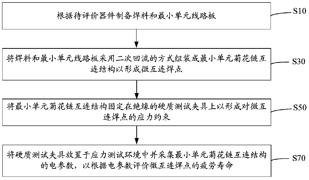
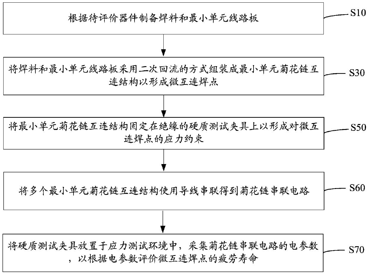
[0040] A fatigue life evaluation method of micro-interconnect solder joints under comprehensive stress, such as figure 1 shown, including the following steps:

[0041] S10: Prepare solder and minimum unit circuit boards according to the device to be evaluated.

[0042] Specifically, suitable solder and minimum unit circuit boards are prepared according to the parameters of the device to be evaluated. For parameters, please refer to the technical data of the device to be evaluated.

[0043] S30: Assemble the solder and the minimum unit circuit board into a minimum unit daisy-chain interconnection structure by means of secondary reflow to form micro-interconnection solder joints. .

[0044] S50: Fix the minimum cell daisy-chain interconnect structure on an insulating rigid test fixture to form stress constraints on the micro-interconnect solder joints.

[0045] S70: Place a hard test fixture in a stress test environment and collect electrical parameters of the smallest unit ...


PUM


Abstract

The invention relates to a method, a device and a system for evaluating a fatigue life of miniature solder joint interconnection under combined stress. The method comprises preparing a solder and a minimum unit circuit board according to a device to be evaluated, assembling the solder and the minimum unit circuit board to form a minimum unit daisy chain interconnection structure through a secondary backflow method so that the miniature solder joint interconnection is formed, fixing the minimum unit daisy chain interconnection structure to an insulative hard test clamp so that stress constraint to the miniature solder joint interconnection is formed, arranging the hard test clamp in a stress test environment, acquiring electrical parameters of the minimum unit daisy chain interconnection structure and evaluating a fatigue life of miniature solder joint interconnection according to the electrical parameters. The method can effectively evaluate a fatigue life of the miniature solder joint interconnection and realize evaluation of the fatigue life of the miniature solder joint interconnections prepared from different solders thereby optimizing the miniature solder joint interconnection structure and materials. Through comparison of fatigue lives of miniature solder joint interconnections prepared from various components, the solder joint structure and materials with best effects are ensured.

Description

technical field [0001] The invention relates to the field of electronic component packaging, in particular to a fatigue life evaluation method, device and system of micro-interconnect solder joints under comprehensive stress. Background technique [0002] High-density packaging micro-interconnect solder joints mainly play the role of mechanical support, signal transmission and heat conduction in electronic assembly technology. Ensuring that solder joints have good mechanical support and electrical connection performance is critical to the reliability of the entire electronic equipment. With the miniaturization of package size, the size of the micro-interconnect pads continues to decrease. The miniaturization of solder joint size leads to significant changes in metallurgical behavior, microstructure formation and evolution during reflow assembly. In particular, the electromigration caused by flip-chip technology makes the interface reaction and microstructure evolution of sol...

Claims


Application Information

Patent Timeline
Patent Type & Authority Patents(China)
IPC IPC(8): G01N27/00G01R31/00
CPCG01N27/00G01R31/00
Inventor 李勋平周斌肖庆中何小琦恩云飞
Owner FIFTH ELECTRONICS RES INST OF MINIST OF IND & INFORMATION TECH
Learn More