Array substrate, production method thereof, touch display panel and display device

An array substrate and touch technology, which is applied in semiconductor/solid-state device manufacturing, optics, instruments, etc., can solve the problems of restricting the ultra-narrow frame of the display panel and the width occupied by the gate drive circuit.

Inactive Publication Date: 2016-09-07
BOE TECH GRP CO LTD +1
View PDF3 Cites 34 Cited by
  • Summary
  • Abstract
  • Description
  • Claims
  • Application Information

AI Technical Summary

Problems solved by technology

However, the gate drive circuit integrated on the array substrate still occupies a certain wi

Method used


Image

  • Array substrate, production method thereof, touch display panel and display device
  • Array substrate, production method thereof, touch display panel and display device
  • Array substrate, production method thereof, touch display panel and display device

Examples


Embodiment Construction

[0032] The specific implementation manners of the array substrate, the manufacturing method thereof, the touch display panel and the display device provided by the embodiments of the present invention will be described in detail below with reference to the accompanying drawings.

[0033] Wherein, the thickness and shape of each film layer in the drawings do not reflect the real proportion of the array substrate, and the purpose is only to illustrate the content of the present invention.

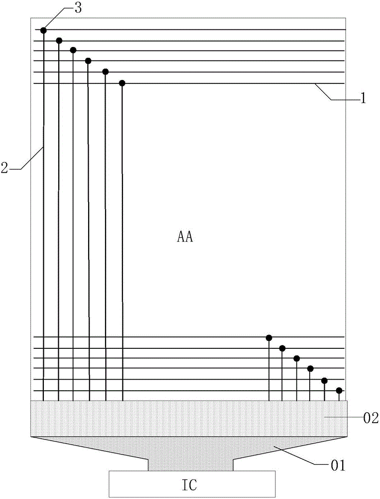
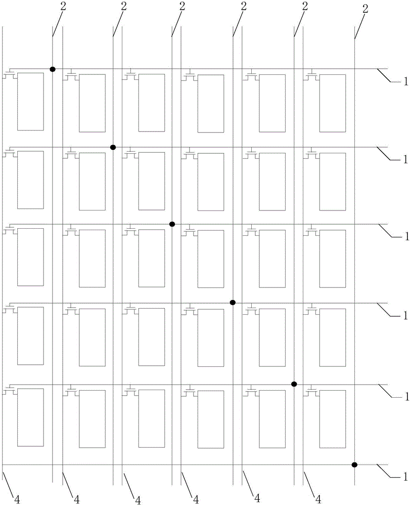
[0034] An embodiment of the present invention provides an array substrate, such as figure 1 As shown, it includes: a base substrate, a plurality of gate lines 1 and a plurality of data lines ( figure 1 not shown in ), and a source drive circuit 01 located in a frame area of ​​the array substrate; each pin of the source drive circuit is directly electrically connected to each data line; it also includes:

[0035] The gate drive circuit 02 located in the same frame area as the source drive cir...


PUM


Abstract

The invention discloses an array substrate, a production method thereof, a touch display panel and a display device. The array substrate comprises a substrate base plate, a plurality of grids lines and a plurality of data lines which are crosswise placed on the substrate base plate and insulating with each other, and a source driving circuit positioned at a frame area of the array substrate, wherein each pin of the source driving circuit is directly and electrically connected with the corresponding data line. The array substrate also comprises a grid driving circuit positioned at the same frame area with the source driving circuit, and metal wires corresponding to the grids in a one-to-one manner and electrically connected with the same, wherein each pin of the grid driving circuit is directly and electrically connected with the corresponding metal wire. As the grid driving circuit and the source driving circuit are both positioned at the same frame area of the array substrate, the grid driving circuit loads scanning signals to the grids via the metal wires, the source driving circuit directly loads gray scale signals to the data lines, thus the screen occupation rate can be greatly improved, the other three sides have ultra-narrow frames even do not have frames, and the user can enjoy unprecedented visual experience and amazing visual effect.

Description

technical field [0001] The present invention relates to the field of display technology, in particular to an array substrate, a manufacturing method thereof, a touch display panel and a display device. Background technique [0002] At present, in order to provide viewers with better visual enjoyment, display products with narrow bezels are the current popular trend. With the rapid development of mobile products, the bezels of display products are getting narrower and narrower. "Borderless" has become a trend in the smartphone industry. The next development trend. [0003] In the prior art, the gate driver circuit is generally formed on the array substrate of the display panel through an array process, that is, the Gate Driver on Array (GOA) process of the array substrate. This integrated process not only saves costs, but also can achieve display The symmetrical and beautiful design on both sides of the panel also saves the bonding area of ​​the IC (Integrated Circuit) and t...

Claims


Application Information

Patent Timeline
IPC IPC(8): H01L27/12G02F1/1362G02F1/1368G02F1/1333H01L21/77
CPCH01L27/12G02F1/1333G02F1/1362G02F1/1368H01L21/77
Inventor 王继国
Owner BOE TECH GRP CO LTD
Why Eureka
Try Eureka