Logic application method for semiconductor heterostructure optoelectronic devices

A technology of optoelectronic devices and application methods, applied in semiconductor devices, electrical components, circuits, etc., can solve the problems of inability to realize gate voltage logic regulation, inability to realize dynamic regulation of semiconductor materials, etc.

Inactive Publication Date: 2019-02-01
TONGJI UNIV
View PDF4 Cites 0 Cited by
  • Summary
  • Abstract
  • Description
  • Claims
  • Application Information

AI Technical Summary

Problems solved by technology

Because in traditional semiconductor materials, the gate voltage cannot realize the dynamic control of the semiconductor material between p-type and n-type, so it is also impossible to realize the logical control of the gate voltage on the optoelectronic (photovoltaic or LED) performance of the semiconductor material.

Method used


Image

  • Logic application method for semiconductor heterostructure optoelectronic devices
  • Logic application method for semiconductor heterostructure optoelectronic devices
  • Logic application method for semiconductor heterostructure optoelectronic devices

Examples


Embodiment

[0033] WS 2 - Black phosphorus heterojunction logic optoelectronic devices

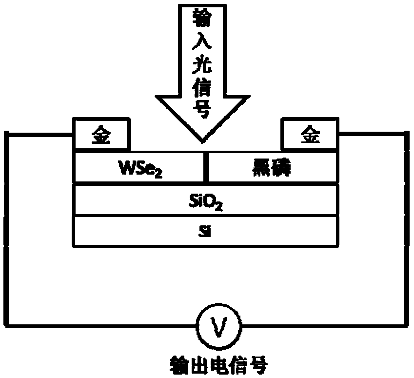
[0034] Such as figure 2 As shown, in this device, the source and drain electrodes are gold, and the channel layer is bipolar WSe 2 The heterojunction of two-dimensional crystal and black phosphorus two-dimensional crystal, the dielectric layer is silicon dioxide, the gate electrode is doped silicon, and the input signal light is irradiated on the WSe 2 - On the black phosphorus heterojunction, the output electrical signal is measured through the source and drain electrodes.

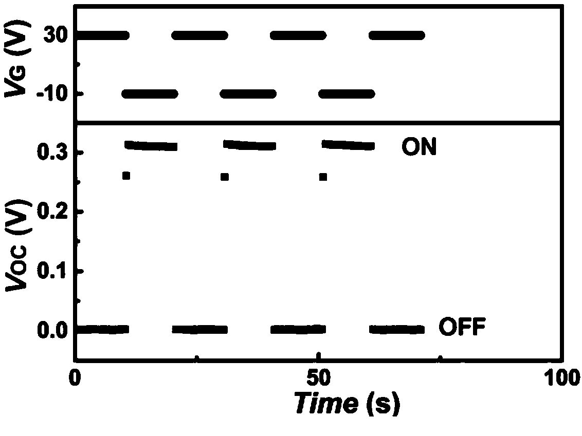
[0035] Such as image 3 As shown, it can be seen that when the gate voltage V G When it is 30V, the generated photovoltaic voltage V OC Close to 0V, at this time the device is in the pinch-off (OFF) state; when the gate voltage V G When it is -10V, the generated photovoltaic voltage V OC About 0.3V, at this time the device is in the ON state.


PUM


Abstract

The invention discloses a logical application method of semiconductor heterostructure optoelectronic device. The device mainly based on the physical properties of nano-semiconductor materials realizes a logic control of grid voltage on the photoelectric conversion property of source drain channel through the structure design of field effect transistor; therefore, the device has the performance of logic photoelectron. The main structure and function of the device are as follows: (1) The device has a similar structure of the field effect transistor; (2) The material of the channel layer is a semiconductor heterojunction material; (3) The semiconductor heterojunction comprises at least one bipolar semiconductor, and carrier type ( type p or n) of the semiconductor can be regulated by the grid; (4) According to the design, a PN junction and a non PN junction can be formed by the grid control of the semiconductor heterojunction. By using the photoelectric conversion property of different heterojunctions, the regulation of grid voltage on the performance of different photoelectric conversion property of channel layer is realized, and the optoelectronic device has a logical function.

Description

technical field [0001] The invention relates to the preparation of a device structure with logic optoelectronic functions by using semiconductor technology. Background technique [0002] In traditional semiconductor materials, such as silicon, its carrier type (p-type or n-type) is mainly realized by element doping. Once doping is formed, it is impossible to dynamically realize the conversion of semiconductor materials between different types of charge doping. . For a silicon pn junction, once formed, the gate voltage can only regulate the carrier concentration of silicon within the range of the pn junction, but cannot regulate the silicon pn junction into a non-pn junction; for an n-type silicon, The gate voltage can only realize the regulation of electron concentration, but cannot regulate n-type silicon into p-type silicon or pn junction, and vice versa. As we all know, the pn junction has different optoelectronic properties from a single p-type or n-type semiconductor ...

Claims


Application Information

Patent Timeline
Patent Type & Authority Patents(China)
IPC IPC(8): H01L33/14H01L33/00
CPCH01L33/005H01L33/14H01L2933/0008
Inventor 马海英张增星李东
Owner TONGJI UNIV
Why Eureka
Try Eureka