Gas Sensors and Sensor Devices
A gas sensor and gas technology, applied in the direction of measuring devices, instruments, scientific instruments, etc., can solve the problem of increased power consumption of the detection circuit
- Summary
- Abstract
- Description
- Claims
- Application Information
AI Technical Summary
Problems solved by technology
Method used
Image
Examples
Embodiment 1
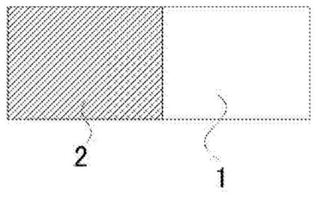
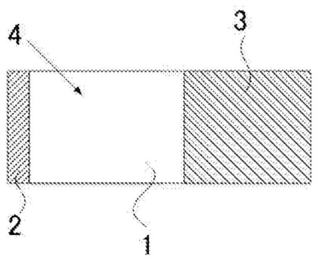
[0145] made as Figure 6A ~ Figure 6C The gas sensor shown. Specifically, the above-mentioned gas sensor was produced by the following method.
[0146]
[0147] A gold electrode (first electrode 2) with a width of 10 mm x a length of 25 mm x an average thickness of 30 nm was formed by vacuum evaporation on a silicon wafer with a thermal oxide film having an average thickness of 1 μm and a width of 12 mm x a length of 50 mm x a thickness of 0.6 mm.
[0148]
[0149] A copper layer having a width of 8 mm×length of 30 mm×an average thickness of 0.5 μm was formed using a vacuum deposition method so as to cover part of the first electrode 2 . Next, by the same method as described in "2. Experimental" of the literature (Pascal Lauque, Marc Bendahan, Jean-Luc Seguin, Kieu An Ngo, Philippe Knauth, Analytica Chimica Acta, 515, (2004), 279-284) Method A copper bromide aqueous solution was used to convert the copper in the copper layer into cuprous bromide to obtain a solid electro...
Embodiment 2
[0158] made as Figure 8A ~ Figure 8C The gas sensor shown. Specifically, the above-mentioned gas sensor was produced by the following method.
[0159]
[0160] A gold electrode (first electrode 2) with a width of 10 mm x a length of 20 mm x an average thickness of 60 nm was formed by vacuum evaporation on a silicon wafer with a thermal oxide film having an average thickness of 1 μm and a width of 12 mm x a length of 50 mm x a thickness of 0.6 mm.
[0161]
[0162] Cuprous bromide (solid electrolyte layer 1 ) of width 8 mm×length 30 mm×average thickness 200 nm was formed using radio frequency magnetron sputtering (RF magnetron sputtering) so as to cover part of the first electrode 2 .
[0163] The conditions of the radio frequency magnetron sputtering method are as follows.
[0164] ·RF power: 100W
[0165] · Sputtering gas: Ar
[0166] Sputtering gas: flow rate 30sccm
[0167] ·Air pressure: 0.5Pa
[0168]
[0169] Furthermore, if Figure 8A As shown, a gold elec...
Embodiment 3
[0179] made as Figure 10 The gas sensor shown. Specifically, the above-mentioned gas sensor was produced by the following method.
[0180]
[0181] Use vacuum evaporation method to form 2 gold electrodes (the first electrode 12 and the first electrode 12 and second electrode 13). The above-mentioned two gold electrodes were provided with a gap of 1 mm between opposing end portions.
[0182]
[0183] A copper layer having a width of 8 mm x a length of 30 mm x an average thickness of 0.5 μm was formed on the above two gold electrodes using a vacuum evaporation method. Next, by the same method as described in "2. Experimental" of the literature (Pascal Lauque, Marc Bendahan, Jean-Luc Seguin, Kieu AnNgo, Philippe Knauth, Analytica Chimica Acta, 515, (2004), 279-284) Method A copper bromide aqueous solution was used to change the copper in the above copper layer to cuprous bromide to fabricate a solid electrolyte layer 11 and obtain a sample.
[0184]
[0185] A copper ...
PUM
| Property | Measurement | Unit |
|---|---|---|
| thickness | aaaaa | aaaaa |
| length | aaaaa | aaaaa |
| thickness | aaaaa | aaaaa |
Abstract
Description
Claims
Application Information
 - R&D
- Intellectual Property
- Life Sciences
- Materials
- Tech Scout
- Unparalleled Data Quality
- Higher Quality Content
- 60% Fewer Hallucinations
Browse by: Latest US Patents, China's latest patents, Technical Efficacy Thesaurus, Application Domain, Technology Topic, Popular Technical Reports.
© 2025 PatSnap. All rights reserved.Legal|Privacy policy|Modern Slavery Act Transparency Statement|Sitemap|About US| Contact US: help@patsnap.com


