Supercharge Your Innovation With Domain-Expert AI Agents!

Chemical mechanical polishing device and method

A chemical machinery and polishing device technology, applied in grinding devices, grinding/polishing equipment, grinding machine tools, etc., can solve the problems of low accuracy of polishing layer thickness, large errors, and reduced measurement precision.

Active Publication Date: 2019-04-26
K C TECH
View PDF6 Cites 0 Cited by
  • Summary
  • Abstract
  • Description
  • Claims
  • Application Information

AI Technical Summary

Problems solved by technology

[0007] However, in the chemical mechanical polishing process, as the polishing layer Le of the wafer W is polished, the polishing pad 11 formed of the worn material is also slightly worn, so that the thickness changes.
In particular, since the adjustment of the target thickness of the polishing layer Le of the wafer allows an error of several tens even hundreds That is, it is very small, so there is a problem that the thickness distribution of the polishing layer Le of the wafer and the polishing end time point of the wafer are likely to be erroneously recognized due to an error caused by a change in the thickness of the polishing pad 11.
[0009] The thickness change value of the polishing pad 11 can be measured by a non-contact optical sensor or a probe elastically supported by a spring, but the measurement precision of the non-contact optical sensor is reduced due to slurry on the polishing pad 11 such as slurry and polishing particles , resulting in large errors, so it is difficult to accurately detect the thickness change value of the polishing pad 11 in real time
[0010] Therefore, conventionally, there is a limitation that the accuracy of the polishing layer thickness of the wafer W becomes low.

Method used


Image

  • Chemical mechanical polishing device and method
  • Chemical mechanical polishing device and method
  • Chemical mechanical polishing device and method

Examples


Embodiment Construction

[0070] Hereinafter, a chemical mechanical polishing device 9 according to an embodiment of the present invention and a polishing head 100 used in the chemical mechanical polishing device 9 will be described in detail with reference to the accompanying drawings. However, in describing the present invention, in order to clarify the gist of the present invention, a detailed description of known functions or structures will be omitted.

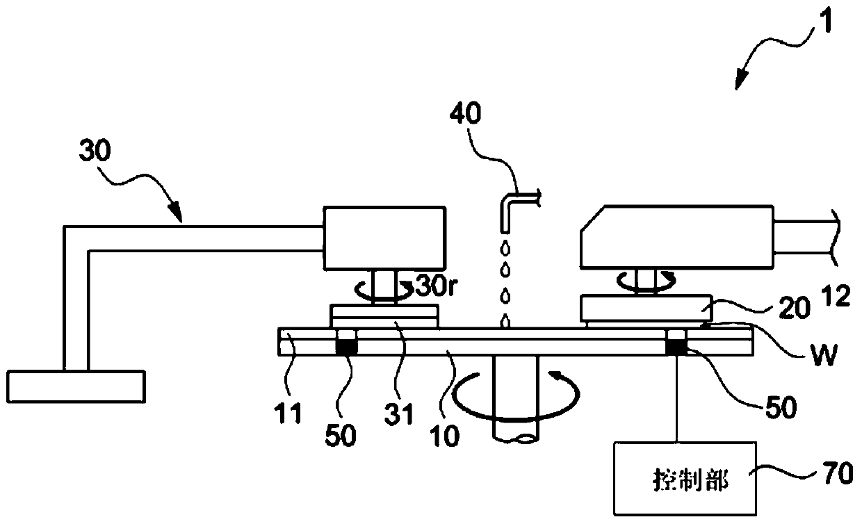
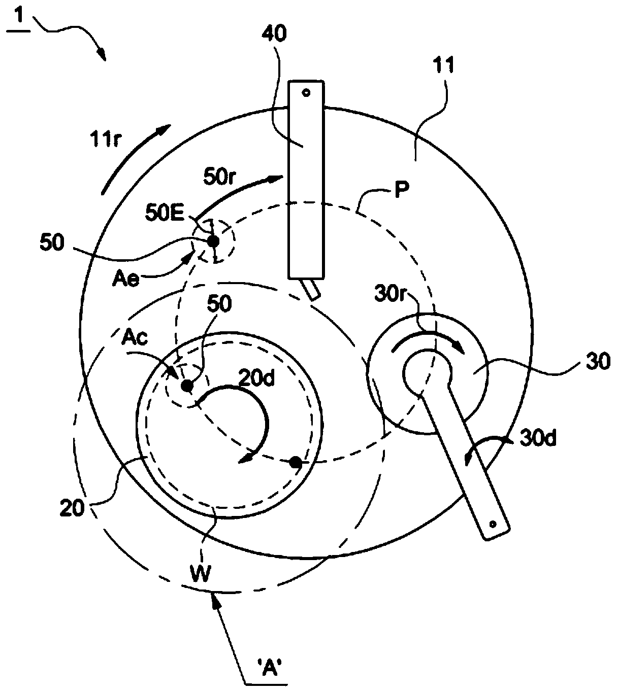
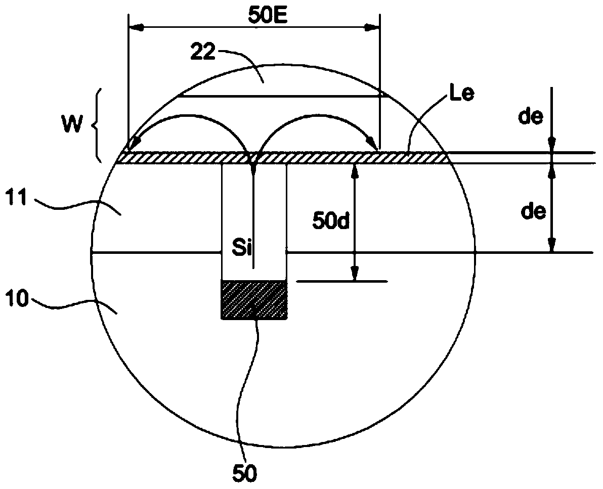
[0071] A chemical mechanical polishing device 9 according to an embodiment of the present invention includes: a polishing plate 10 covered by a polishing pad 11 that contacts the polishing surface of the wafer W; , and make the wafer W rotate; the eddy current sensor 50 applies an eddy current to detect the thickness of the polishing layer of the wafer W and receives an output signal from the polishing layer; and the control unit 90 applies an alternating current to the eddy current sensor 50, and from The output signal received by the eddy curren...


PUM


Abstract

The present invention relates to a chemical mechanical polishing apparatus. The chemical mechanical polishing apparatus comprises: a grinding surface plate whose upper surface is coated with a polishing pad; a polishing head for contacting the plate of a wafer to press the same during the chemical mechanical polishing process, having a retainer ring including a first member made of conductive substances with a first end surface and a second end surface having a different height around the wafer and a second member contacting the polishing pad during the chemical mechanical polishing process, made of non-conductive substances at the lower part of the first member; a width sensor applying current signals to the wafer to acquire information about the width of the paper; and a control unit for acquiring the width of a wafer polishing layer by reflecting the information about the width of the polishing pad from a third output signal, by acquiring the third output signal from the polishing layer of the wafer from the parts of the width sensor and acquiring information about the width of the polishing pad from a second output signal, at the first and second ends, from parts of the width sensor. Therefore, by reflecting changes in the width of the polishing pad on the width of the conductive layer of the wafer computed from eddy current output signals, the chemical mechanical polishing apparatus is capable of precisely measuring the width of the conductive layer of the wafer, considering the abrasion loss of the polishing pad.

Description

technical field [0001] The present invention relates to a chemical mechanical polishing device and method, in more detail, to a chemical mechanical polishing device that can reflect the thickness change of the polishing pad in the chemical mechanical polishing process to accurately obtain the thickness of the wafer polishing layer formed by conductive materials and methods. Background technique [0002] In general, the chemical mechanical polishing (CMP) process refers to rotating a rotating polishing plate in a state of contacting a substrate such as a wafer, and performing mechanical polishing to flatten the surface of the substrate to achieve Pre-specified thickness of the process. [0003] For this, as figure 1 As shown, the chemical mechanical polishing apparatus 1 rotates while making the polishing pad 11 cover the upper state of the polishing plate 12, and uses the polishing head 20 to press the wafer W on the surface of the polishing pad 11 and rotates, thereby pol...

Claims


Application Information

Patent Timeline
Patent Type & Authority Patents(China)
IPC IPC(8): B24B37/10B24B37/32B24B37/013B24B49/02B24B49/10
CPCB24B37/013B24B37/10B24B37/32B24B49/02B24B49/105
Inventor 金钟千金旻成任桦爀金志郁
Owner K C TECH
Features
  • R&D
  • Intellectual Property
  • Life Sciences
  • Materials
  • Tech Scout
  • Unparalleled Data Quality
  • Higher Quality Content
  • 60% Fewer Hallucinations
Learn More