A display substrate, display panel, display device and display method thereof

A display panel and display substrate technology, applied in the field of multi-view field display, can solve the problems of lower resolution, lower quality of dual-view display images, display image distortion, etc.

Active Publication Date: 2021-08-17
BEIJING BOE OPTOELECTRONCIS TECH CO LTD +1
View PDF7 Cites 0 Cited by
  • Summary
  • Abstract
  • Description
  • Claims
  • Application Information

AI Technical Summary

Problems solved by technology

[0004] However, there is a serious problem in the existing dual-view display panels: as shown in Figure 1(a) and Figure 1(b), the pixel units 10 in the dual-view display panels in the prior art The length along the row direction is equal to the length along the column direction. For a dual-view display panel and an ordinary display panel of the same size, when the size of the pixel unit is the same, since the number of pixel units set in the same row is the same, the same The number of dual-view pixel units 11 in a row of dual-view display panels is half of the number of pixel units 10 in an ordinary display panel, that is, the number of left-view pixel units 111 or right-view pixel units 112 in the same row is equal to that of an ordinary display panel. half of the number of pixel units 10 in the middle, so if the image information in the ordinary display panel is input to the left-view pixel unit 111 or the right-view pixel unit 112, it will cause the display screen distortion of the left-view field or the right-view field ; To ensure that the displayed image is not deformed, it is necessary to remove half of the image information in the ordinary display panel, which will cause the resolution of the image displayed in the left field of view or the image displayed in the right field of view to be reduced to 1 / 1 of the resolution of the ordinary display image 2, which will greatly reduce the picture quality of dual-field display

Method used


Image

  • A display substrate, display panel, display device and display method thereof
  • A display substrate, display panel, display device and display method thereof
  • A display substrate, display panel, display device and display method thereof

Examples


Embodiment Construction

[0043] The following will clearly and completely describe the technical solutions in the embodiments of the present invention with reference to the accompanying drawings in the embodiments of the present invention. Obviously, the described embodiments are only some of the embodiments of the present invention, not all of them. Based on the embodiments of the present invention, all other embodiments obtained by persons of ordinary skill in the art without making creative efforts belong to the protection scope of the present invention.

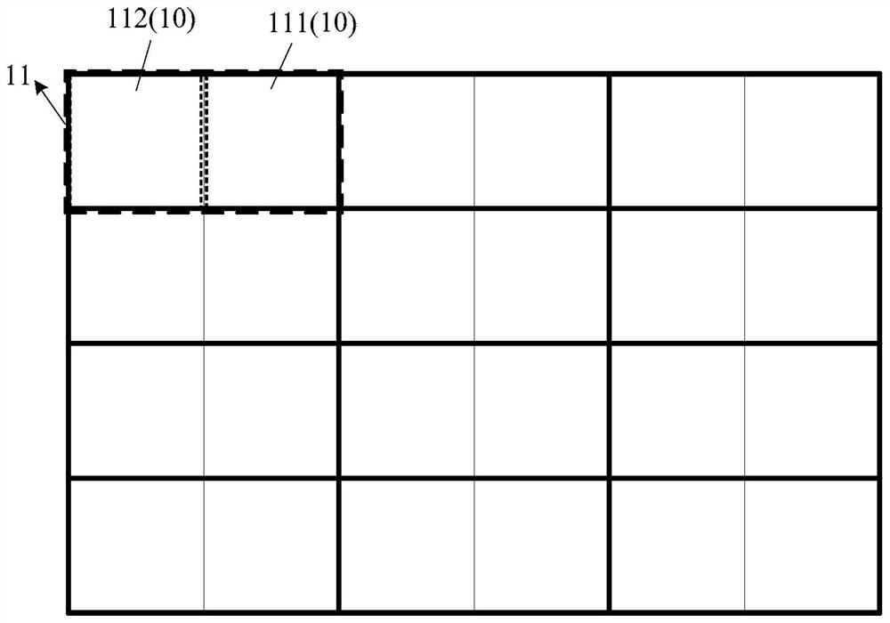
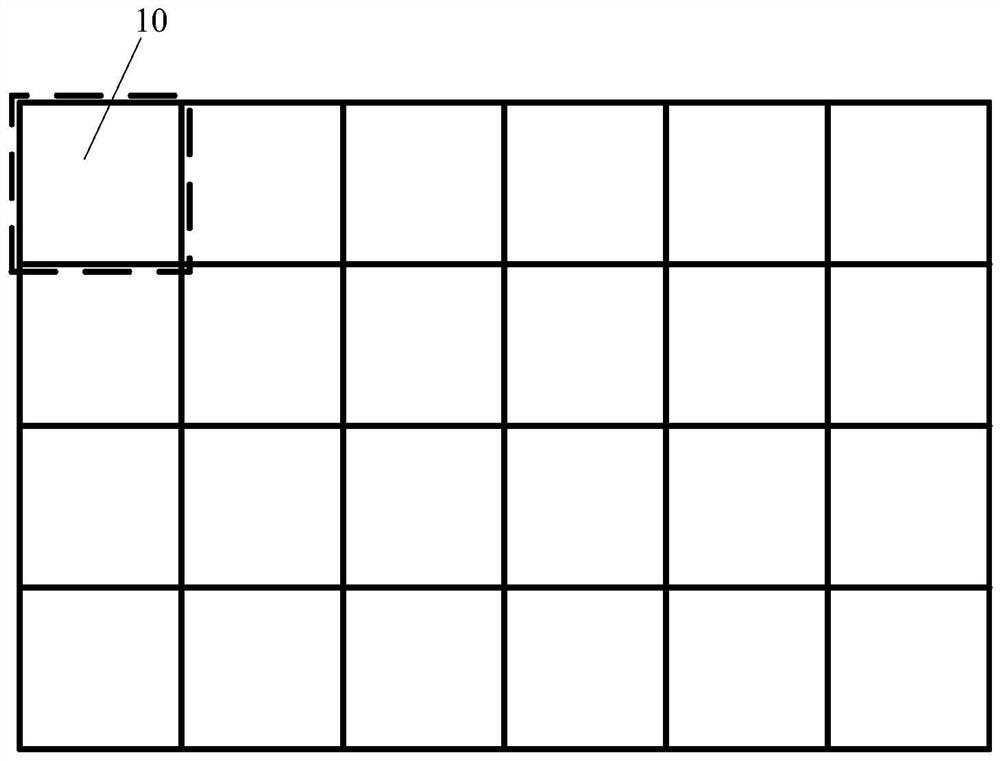
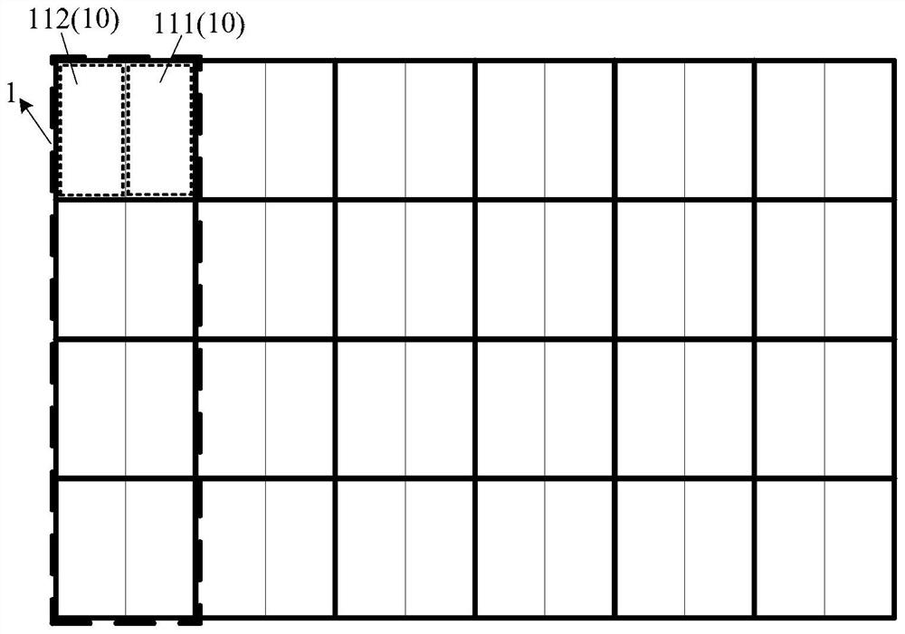
[0044] An embodiment of the present invention provides a display substrate, as shown in Fig. 2(a) and Fig. 2(b), comprising: a plurality of display groups 1 arranged repeatedly along the row direction, and each display group 1 includes: n columns of different viewing For the pixel units 10 in the field, the ratio of the length of each pixel unit 10 along the row direction to the length along the column direction is 1 / n; wherein, n≥2, n is a positi...


PUM


Abstract

Embodiments of the present invention provide a display substrate, a display panel, a display device and a display method thereof, which relate to the technical field of multi-view field display, and can avoid distortion of a display image without reducing the resolution of the display image. The display substrate includes: a plurality of display groups repeatedly arranged along the row direction, each display group includes: n columns of pixel units with different fields of view, the ratio of the length of each pixel unit along the row direction to the length along the column direction is 1 / n; wherein, n≥2, n is a positive integer. Used in multi-field display substrates.

Description

technical field [0001] The present invention relates to the technical field of multi-view field display, in particular to a display substrate, a display panel, a display device and a display method thereof. Background technique [0002] With the development of display technology, in order to meet the needs of consumers of different groups and hobbies to obtain different display screen information from different viewing fields, so as to enhance the unique visual experience, multi-viewing fields (for example: double viewing field, triple viewing Field, etc.) display devices also came into being. [0003] Taking a dual-view display device as an example, a dual-view display refers to a display technology in which different images can be seen from different positions relative to the display screen at the same time. This dual-view display technology usually uses the parallax barrier method. Utilizing the light-shielding stripes of the double-viewing-field light-shielding layer (g...

Claims


Application Information

Patent Timeline
Patent Type & Authority Patents(China)
IPC IPC(8): G09F9/302G09F9/35H01L27/32
CPCG09F9/302G09F9/35H10K59/00G09G3/003G09G3/3225G09G3/3648G02F1/1323G02F1/133504G02F1/133512H10K59/353
Inventor 罗兴友李月陈希
Owner BEIJING BOE OPTOELECTRONCIS TECH CO LTD
Why Eureka
Try Eureka