

Array substrate and display panel
A technology for array substrates and display areas, applied to static indicators, instruments, nonlinear optics, etc., to achieve the effect of protecting against short circuits
- Summary
- Abstract
- Description
- Claims
- Application Information
AI Technical Summary
Problems solved by technology
Method used
Image

Examples
Embodiment Construction
[0023]An array substrate and a display panel of the present invention will be described in more detail below in conjunction with the schematic diagrams, which show preferred embodiments of the present invention. It should be understood that those skilled in the art can modify the present invention described here and still realize the advantages of the present invention. Favorable effect. Therefore, the following description should be understood to be widely known to those skilled in the art, and not as a limitation to the present invention.
[0024]The terms used in the embodiments of the present invention are only for the purpose of describing specific embodiments, and are not intended to limit the present invention. The singular forms of "a", "the" and "the" used in the embodiments of the present invention and the appended claims are intended to include plural forms, unless the context clearly indicates other meanings.
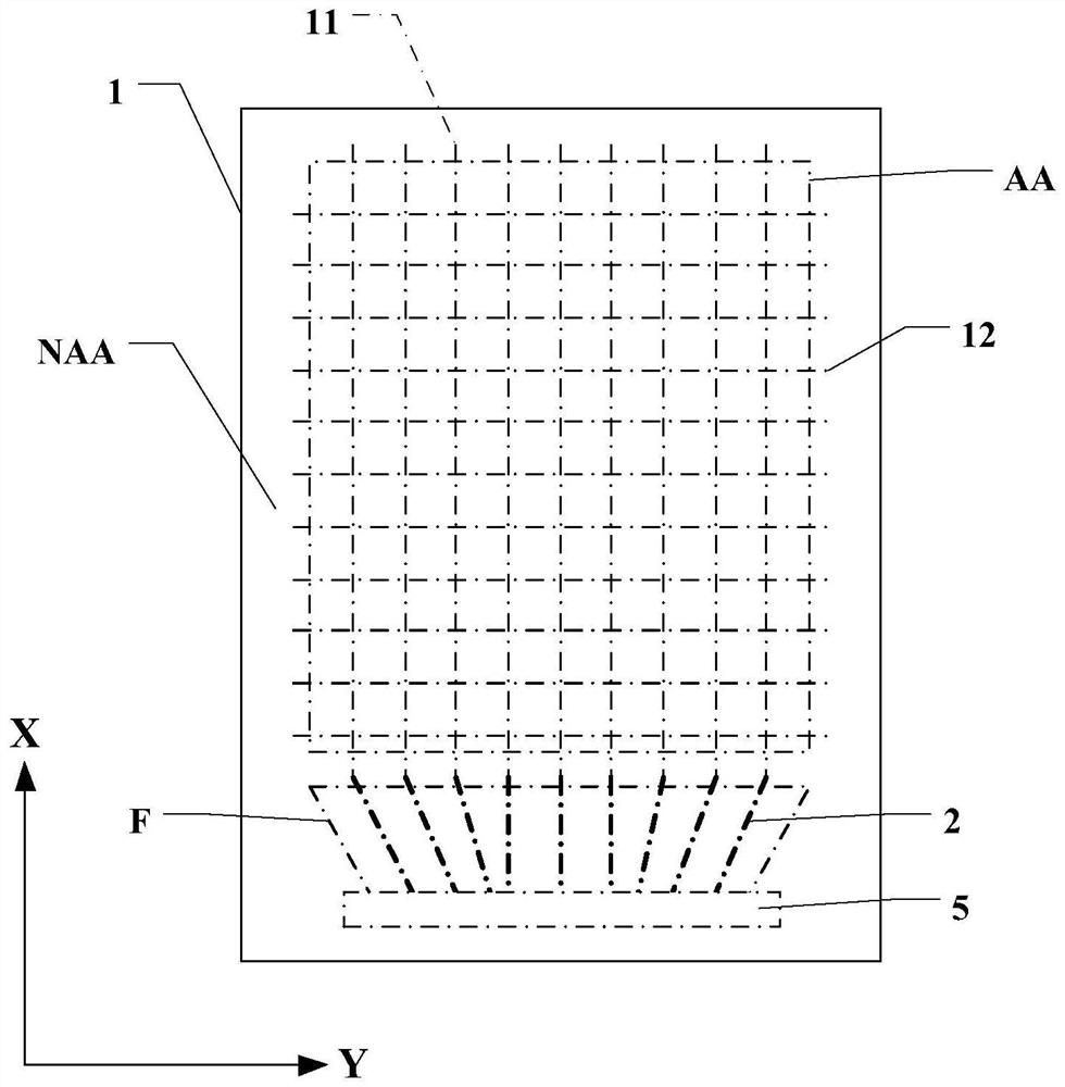
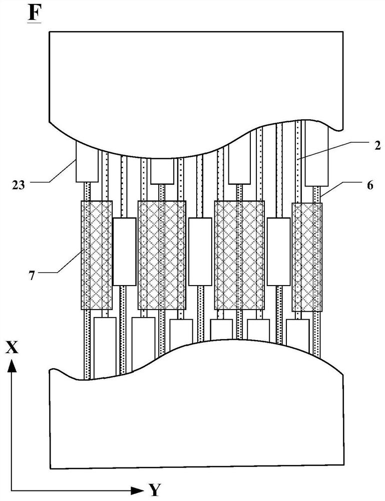
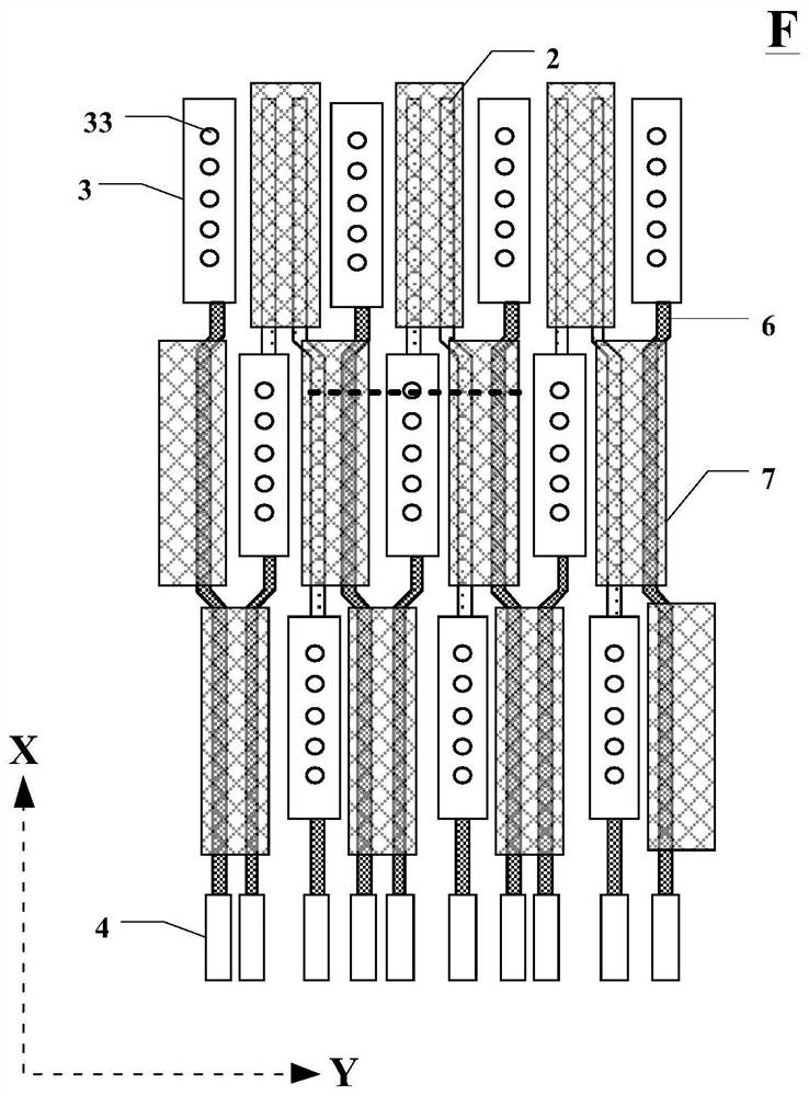
[0025]The present invention provides an array substrate having a d...
PUM
 Abstract
Description
Claims
Application Information