A multi-quantum well structure and its light-emitting diode

A multi-quantum well structure and light-emitting diode technology, applied in semiconductor devices, electrical components, circuits, etc., can solve the problems of light efficiency loss, increase the thickness of the cover layer, and cannot change the energy band distortion of the active layer, so as to improve the crystal quality , Improve the effect of high voltage and large electron overflow

Active Publication Date: 2019-05-14
ANHUI SANAN OPTOELECTRONICS CO LTD
View PDF5 Cites 0 Cited by
  • Summary
  • Abstract
  • Description
  • Claims
  • Application Information

AI Technical Summary

Problems solved by technology

[0003] At present, in order to improve the resistance of the epitaxial barrier crystal layer to high current and alleviate and overcome the influence of the Droop effect, most epitaxial structure designs adopt the design of an optimized electron blocking layer after the active layer, such as AlGaN with a graded Al composition. Single layer, or electron blocking layer of superlattice structure, such as AlGaN / GaN SLs, AlN / GaN SLs, and AlN / AlGaNSLs, but the design of these epitaxial barrier crystal layer structures cannot change the energy band distortion inside the active layer, While improving the electron overflow, it also increases the thickness of the cap layer, resulting in the loss of light efficiency

Method used


Image

  • A multi-quantum well structure and its light-emitting diode
  • A multi-quantum well structure and its light-emitting diode
  • A multi-quantum well structure and its light-emitting diode

Examples


Embodiment 1

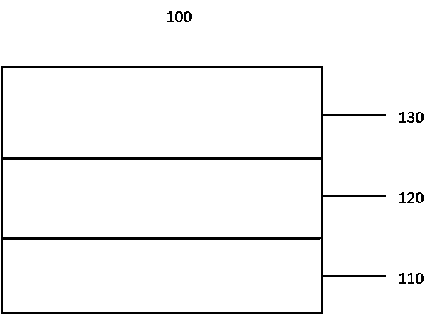
[0032] See attached figure 1 , a multi-quantum well structure 100, comprising a stress release layer 110, an electron collection layer 120, and a light emitting layer 130, the light emitting layer 130 comprising several alternately grown barrier layers and potential well layers, wherein at least one barrier layer is GaN / Al x In y Ga (1-x-y) N / GaN structure, 0x1 N / GaN structure, where, 0.05≤x 1 ≤0.20, further 0.1≤x 1 ≤0.15, its thickness is 140Å~190Å, while Al x1 The thickness of the N layer is 20Å~30Å.

[0033] The electron collection layer 120 includes several alternately stacked GaN barrier layers and InGaN well layers, and the number of cycles is 3 to 6. In order to slow down the electron mobility, an AlGaN layer is inserted into the last GaN barrier layer of the electron collection layer 120 to form a GaN / AlGaN / GaN structure of the final barrier layer, the insertion of the AlGaN layer not only improves the low efficiency of the internal quantum well and the Droop e...

Embodiment 2

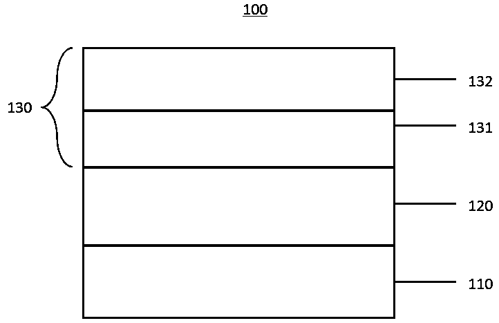
[0038] See attached image 3 , the multi-quantum well structure 100 includes a stress release layer 110, an electron collection layer 120, and a light-emitting layer 130, and the light-emitting layer 130 includes several alternately grown barrier layers and potential well layers, wherein at least one barrier layer is GaN / Al x In y Ga (1-x-y) N / GaN structure, 0x2 In y2 Ga (1-x2-y2) N / GaN structure, the barrier layer of the second light-emitting layer 132 is a GaN structure, 0x2 Ga (1-x2) N / GaN structure, where 0.02≤x2≤0.06. The period number of the first light-emitting layer 131 is 4-8, and the period number of the second light-emitting layer 132 is 5-10.

[0039] Setting the barrier layer in the first light-emitting layer 131 to multiple groups of low Al components can first slow down the phenomenon of electron overflow under high current density, greatly increase the probability of effective recombination radiation of electron holes in the light-emitting layer 130, and i...

Embodiment 3

[0044] See attached Figure 5 , the multi-quantum well structure 100 layer includes a stress release layer 110, an electron collection layer 120, an electron trench layer 140, and a light-emitting layer 130, and the light-emitting layer 130 includes several alternately grown barrier layers and potential well layers, wherein at least one potential barrier layer is GaN / Al x In y Ga (1-x-y) N / GaN structure, 0x2 In y2 Ga (1-x2-y2) N / GaN structure, the potential well layer is an InGaN structure; the last potential barrier layer of the second light emitting layer 132 is the last potential barrier layer is GaN / Al x1 N / GaN structure, where, 0.1≤x1≤0.15, its thickness is 80Å~120Å, and Al x1 The thickness of the N layer is 20Ř30Å, the barrier layers of the remaining second light emitting layer 132 are GaN structures, and the potential well layers are all InGaN structures. Preferably, the barrier layer of the first light-emitting layer 131 is GaN / Al x2 Ga (1-x2) N / GaN structure,...


PUM


Abstract

The invention belongs to the technical field of semiconductors, and in particular relates to a multi-quantum well structure and a light-emitting diode thereof. The multi-quantum well structure includes a stress release layer, an electron collection layer and a light-emitting layer, and the light-emitting layer includes several alternately grown barrier layers. and well layers, at least one of which is GaN / Al x In y Ga (1‑x‑y) N / GaN structure, 0<x≤1, 0≤y<1, and the remaining barrier layers are GaN structures; the light-emitting diode includes at least one substrate, and a buffer layer, an N-type layer, and a multi-quantum layer sequentially located on the substrate Well structure layer, electron blocking layer, P-type layer and P-type contact layer. In the present invention, a barrier layer with a band gap higher than GaN is set in each layer of the multi-quantum well structure, which is equivalent to dispersing the electron blocking layer in the existing structure in the multi-quantum well structure layer, so as to disperse and block electrons. The effect of enhancing the electron blocking effect, improving the phenomenon of electron overflow under high current density and the resulting Droop effect, and improving the light-emitting efficiency of the light-emitting diode.

Description

technical field [0001] The invention belongs to the technical field of semiconductors, and in particular relates to a multi-quantum well structure and a light-emitting diode thereof. Background technique [0002] As the LED industry is becoming more and more perfect, the design and development of LED white light lighting products with high current density and high brightness devices are becoming more and more intense. At the same time, in order to increase the demand for market competitiveness, under the premise of maintaining product performance, especially the brightness level, the degree of gradually reducing the size is becoming more and more intense, which further increases the demand for high current density tolerance in the design of the epitaxial layer structure, especially the need to overcome The impact of the Droop effect. [0003] At present, in order to improve the resistance of the epitaxial barrier crystal layer to high current and alleviate and overcome the ...

Claims


Application Information

Patent Timeline
Patent Type & Authority Patents(China)
IPC IPC(8): H01L33/06H01L33/22H01L33/32
CPCH01L33/06H01L33/22H01L33/32H01L33/12H01L33/0075
Inventor 江汉蓝永凌黄文宾宋长伟黄理承寻飞林林兓兓蔡吉明张家宏
Owner ANHUI SANAN OPTOELECTRONICS CO LTD
Why Eureka
Try Eureka