Coplanar bonding structure and preparation method thereof

A bonding structure and coplanar technology, applied in the field of coplanar bonding structure and its preparation, can solve the problems of inability to guarantee reliable connection of bonding frame, mechanical damage and destruction of lead pads, etc.

Active Publication Date: 2019-05-31
上海烨映微电子科技股份有限公司
View PDF7 Cites 0 Cited by
  • Summary
  • Abstract
  • Description
  • Claims
  • Application Information

AI Technical Summary

Problems solved by technology

At present, both Through Silicon Via (TSV) and Through-wafer Interconnects (TWI) are effective ways to realize the vertical interconnection of 3D stacked chips. However, at the wafer level, these two technologies However, it is difficult to achieve simultaneous bonding of the bonding frame of the device vacuum or hermetic package and the pad of the electrical interconnection with the package cap, because there is a problem of coplanar bonding in the wafer-level bonding process
[0004] In fact, after the silicon wafer has gone through multiple repeated semiconductor manufacturing processes, its functional areas (such as the movable structure, the lead pads of the two functional areas of the support structure, and the functional area of ​​the bonding frame, etc.) are no longer on the same plane. In 3D packaging, it is often necessary to realize the vertical extraction of signals from the lead pads through bonding. Since the plane of the bonding frame is often lower than the plane of the lead pads at this time, when ensuring the reliable connection of the bonding frame (such as vacuum or Hermetic package) is easy to cause mechanical damage or even damage to the lead pads, or in order to achieve the electrical vertical interconnection of the lead pads, the reliable connection of the bonding frame cannot be guaranteed

Method used


Image

  • Coplanar bonding structure and preparation method thereof
  • Coplanar bonding structure and preparation method thereof
  • Coplanar bonding structure and preparation method thereof

Examples


preparation example Construction

[0120] The invention provides a method for preparing a coplanar bonding structure, the preparation method comprising the following steps:

[0121] a) Provide a device structure to be bonded, the device structure includes at least two defined functional areas, wherein each of the functional areas has a surface to be extracted, and at least two of the surfaces to be extracted are located at different heights on flat surface;

[0122] b) Leading each of the faces to be led out to a plane of the same height through a laminated structure formed alternately by insulating layers and metal layers to form each bonding lead-out face, so as to obtain the coplanar bonding structure.

[0123] Specifically, using the stacked structure to lead each of the faces to be extracted to the same plane means that the deposited material at the lower position is lifted in the longitudinal direction by forming the stacked structure during the device formation process. High enough to be integrated with...

Embodiment 1

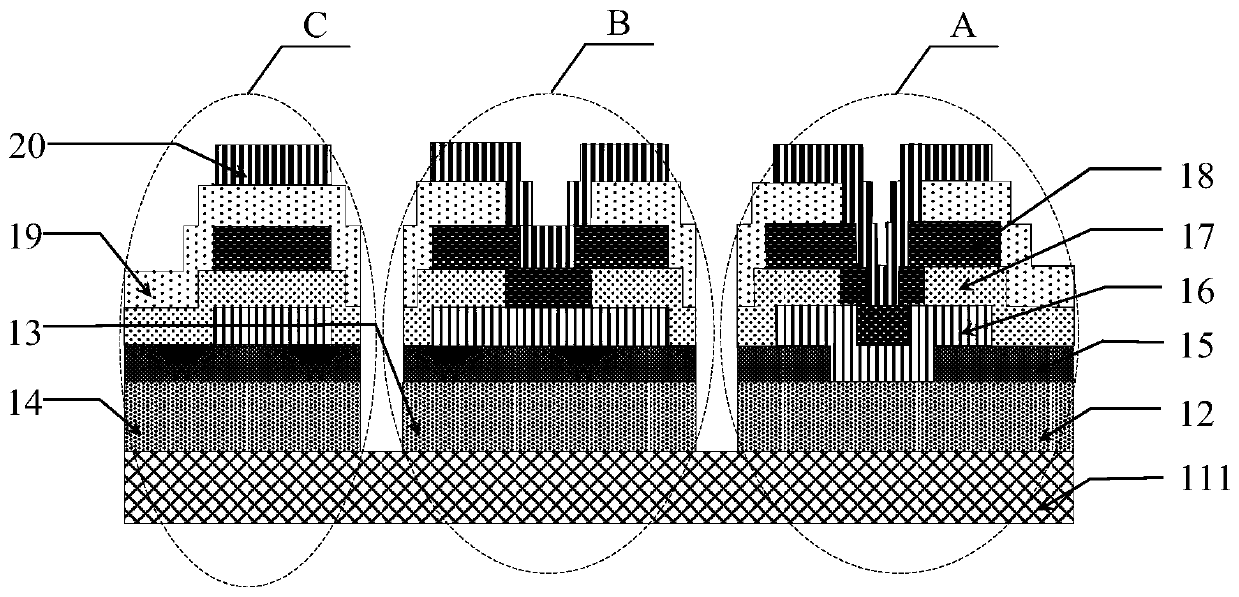
[0135] Such as Figure 1-12 As shown, this embodiment 1 provides a method for preparing a coplanar bonding structure, and the preparation method includes the following steps:

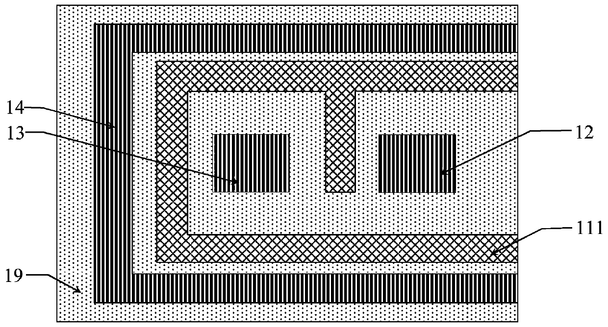
[0136] Such as figure 1 , figure 2 as well as Figure 5 As shown, step 1) is performed to provide a substrate 11, on which a first functional area A, a second functional area B and a third functional area C are defined independently of each other, wherein the third functional area The shape of C is a closed ring structure (the schematic diagram of its partial structure is shown in the figure), wherein, the ring structure can be a square ring or a ring, depending on specific needs, and no specific limitation is made here. A functional area A and the second functional area B are sequentially arranged in the ring structure;

[0137] Specifically, the substrate 11 provides an initial plane of the same height, and the substrate 11 can be any desired structure. In addition, in this embodiment, the second...

Embodiment 2

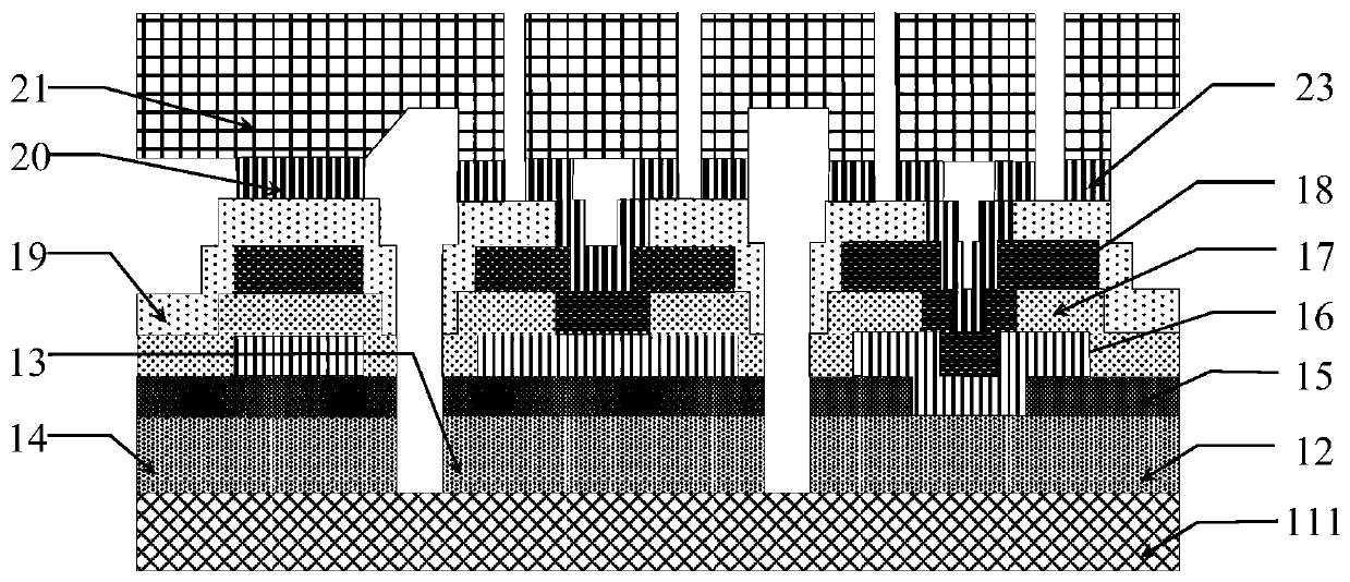
[0162] Such as Figures 13 to 14 As shown, this embodiment 2 provides a method for preparing a coplanar bonding structure. The difference between the coplanar bonding structure in this embodiment 2 and the coplanar bonding structure in embodiment 1 includes the setting of the stacked structure, Other structures and preparation steps are the same or similar to those of Embodiment 1. Refer to the relevant drawings of Embodiment 1. The preparation method includes the following steps:

[0163] 1) Provide a substrate 11 on which a first functional area, a second functional area and a third functional area are defined;

[0164] 2) Depositing a first insulating layer 15 on the substrate 11, and etching at the position corresponding to the first functional area, exposing part of the substrate to form a first electrode lead-out window 151 with a predetermined width, so as to obtain The surface to be led out of the first functional area;

[0165] 3) Deposit the first metal layer 16 on...


PUM


Abstract

The invention provides a coplanar bonding structure and a preparation method thereof. The preparation method comprises the following steps: a, providing a device structure to be bonded, wherein the device structure comprises at least two defined function areas, each function area is provided with a face to be drawn out, and the at least two faces to be drawn out are disposed at planes at different heights; and b, drawing each face to be drawn out to planes at the same height to form each bonding drawn-out face so as to obtain the coplanar bonding structure through a lamination structured alternatively formed by an insulation layer and a metal layer. According to the invention, the coplanar bonding structure can solves the problem that the bonding planes in vacuum or air-tight packaging are not at the same height; the internal structure of the vacuum or air-tight packaging is directly vertically interconnected with the outside of the device; and electrical conduction of insulation and lead wire pads of a bonding frame is realized. The coplanar bonding structure only requires to modify patterns at corresponding positions of masks and does not require additional operation procedures, thereby greatly saving the manufacturing cost and improving the production efficiency.

Description

technical field [0001] The invention relates to the fields of micro-electromechanical systems and packaging, in particular to a coplanar bonding structure and a preparation method thereof. Background technique [0002] Micro Electro Mechanical System (MEMS) is a micro-device or system that integrates micro-mechanisms, micro-sensors, micro-actuators, and signal processing and control circuits, up to interfaces, communications, and power supplies. MEMS technology is developing into a huge industry. However, to realize the commercialization and marketization of MEMS, more in-depth and systematic research on MEMS packaging is required. The packaging form of MEMS products is the key factor to successfully market them, and also a key factor in the design and manufacture of MEMS. The best packaging can make MEMS products play their due functions. The main function of MEMS device packaging is to provide mechanical support and environmental protection for the chip, so as not to be d...

Claims


Application Information

Patent Timeline
Patent Type & Authority Patents(China)
IPC IPC(8): B81C1/00B81B7/00
CPCB81B7/0032B81C1/00261
Inventor 熊斌梁亨茂刘松徐德辉
Owner 上海烨映微电子科技股份有限公司
Why Eureka
Try Eureka