A circuit for correcting operational amplifier offset by successive approximation
What is AI technical title?
AI technical title is built by PatSnap AI team. It summarizes the technical point description of the patent document.
A technique of successive approximation and circuit, which is applied in the direction of improving the amplifier to reduce the influence of noise, etc., and can solve the problems of increasing the correction time and long startup time of the op amp
Active Publication Date: 2020-07-07
西安华泰半导体科技有限公司
View PDF9 Cites 0 Cited by
Summary
Abstract
Description
Claims
Application Information
AI Technical Summary
This helps you quickly interpret patents by identifying the three key elements:
Problems solved by technology
Method used
Benefits of technology
Problems solved by technology
At present, there are methods to solve the problems caused by the above solutions, but if the accuracy of offset correction is to be improved, the correction time will inevitably be increased, which brings about the problem of too long start-up time of the op amp
Method used
Image
Click on the blue label to locate the original text in one second.
Reading with bidirectional positioning of images and text.
Examples
Embodiment 1
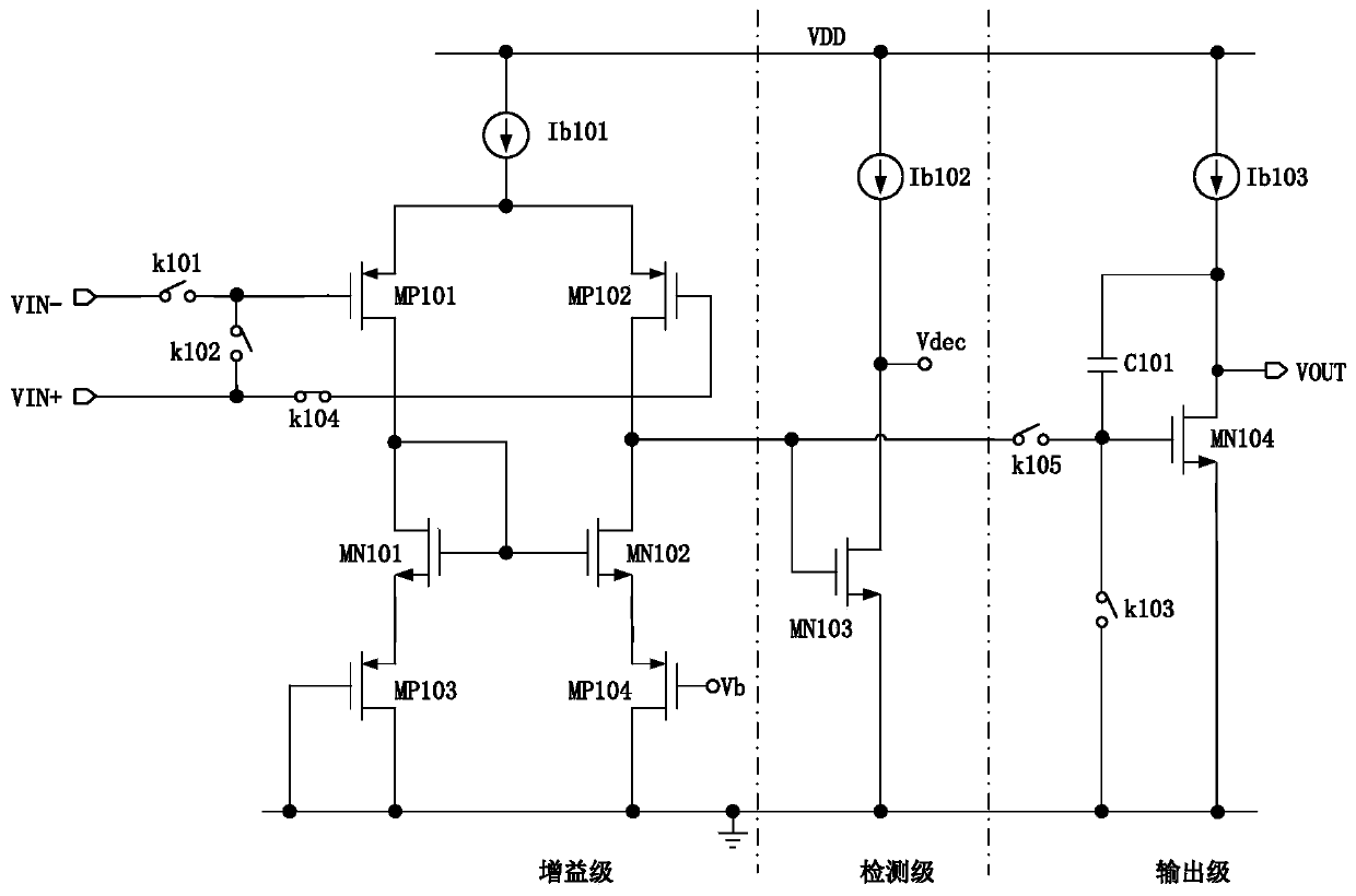
[0024] see figure 2 , is the circuit diagram of the main module of the operational amplifier of the present invention, including PMOS transistor MP101, PMOS transistor MP102, PMOS transistor MP103, PMOS transistor MP104, NMOS transistor MN101, NMOS transistor MN102, NMOS transistor MN103, NMOS transistor MN104, current source Ib101, current source Ib102, current source Ib103, switch k101, switch k102, switch k103, switch k104, switch k105, capacitor C101.
[0025] The operational amplifier is divided into three sections: gain stage, detection stage, and output stage.
[0026] The gain stage includes: PMOS transistor MP101, PMOS transistor MP102, PMOS transistor MP103, PMOS transistor MP104, NMOS transistor MN101, NMOS transistor MN102, current source Ib101, switch k101, switch k102, switch k104. The non-inverting input terminal is connected to the gate of the PMOS transistor MP102 through k104, the inverting input terminal is connected to the gate of the PMOS transistor MP10...
Embodiment 2
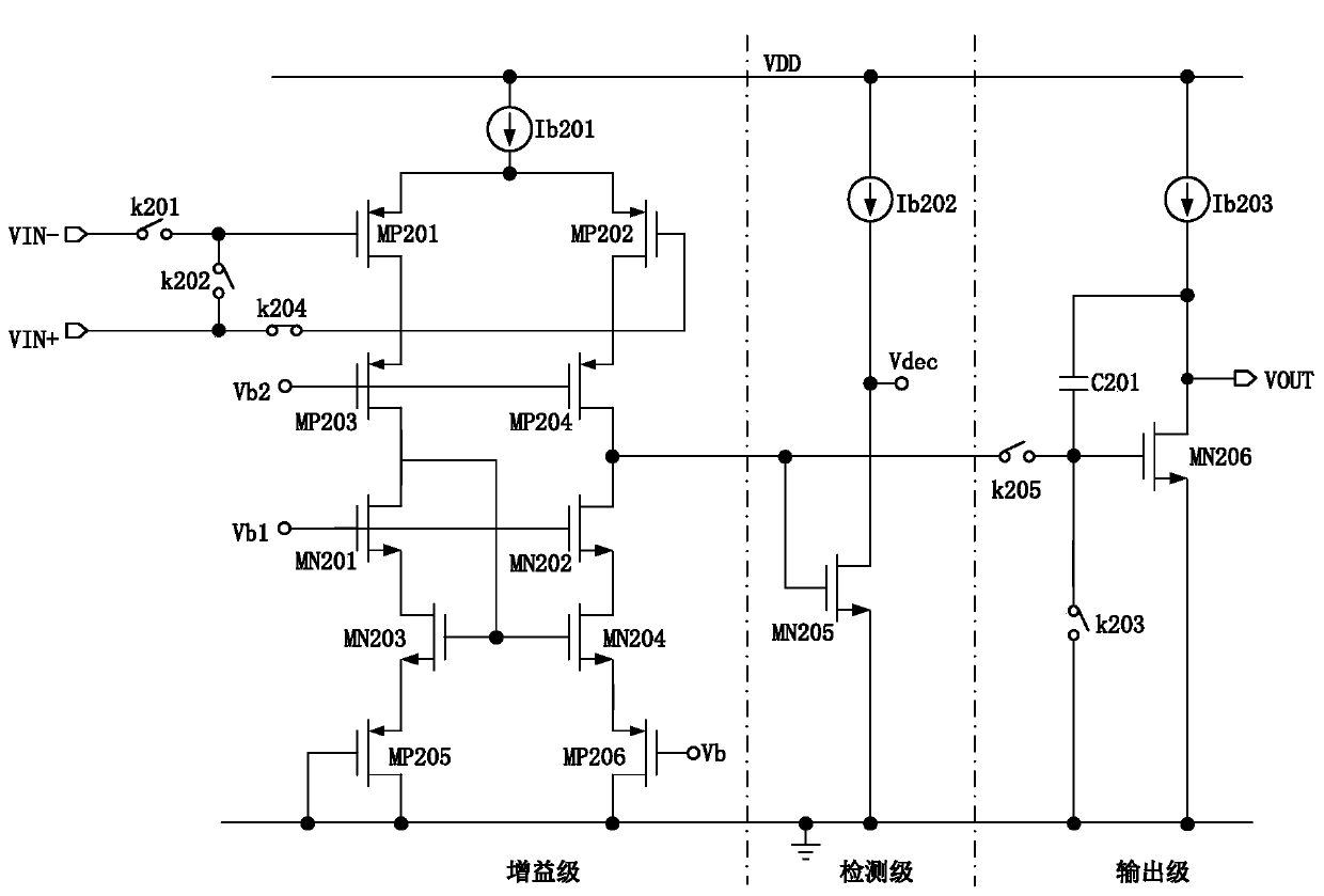
[0036] The structure of the operational amplifier in this embodiment is the same as that in Embodiment 1, and the gain stage in the main module of the operational amplifier is replaced with a telescopic operational amplifier structure.
[0037] see image 3 , is the circuit diagram of the main module of the operational amplifier of the present invention, including PMOS transistor MP201, PMOS transistor MP202, PMOS transistor MP203, PMOS transistor MP204, PMOS transistor MP205, PMOS transistor MP206, NMOS transistor MN201, NMOS transistor MN202, NMOS transistor MN203, NMOS transistor MN204, NMOS transistor MN205, NMOS transistor MN206, current source Ib201, current source Ib202, current source Ib203, switch k201, switch k202, switch k203, switch k204, switch k205, capacitor C201.
[0038] The operational amplifier is divided into three sections: gain stage, detection stage, and output stage.
[0039] The gain stage includes: PMOS transistor MP201, PMOS transistor MP202, PMOS t...
PUM
Abstract
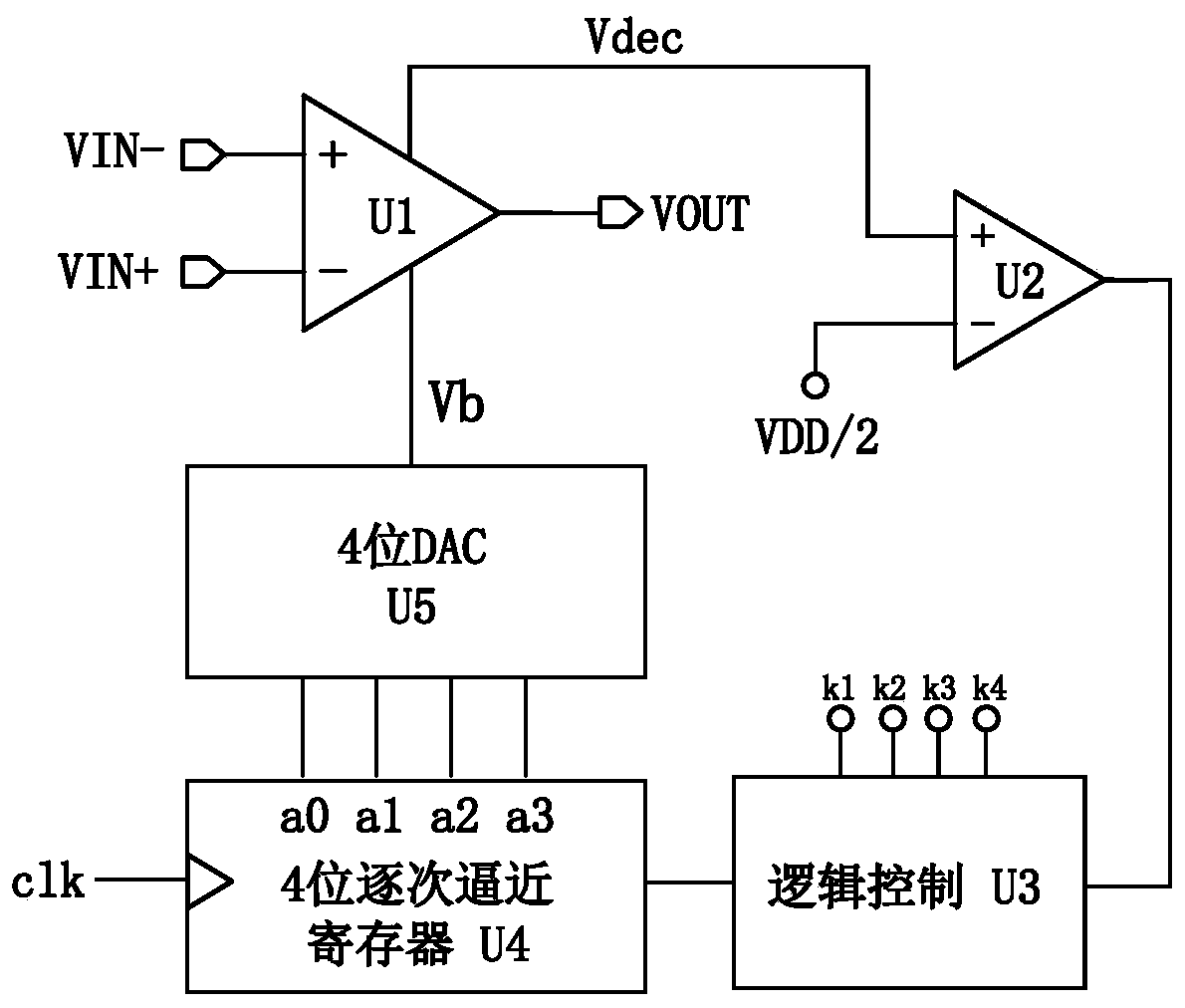
The invention discloses a circuit for calibrating operational amplifier imbalance in a successive approximation register mode. The circuit comprises an operational amplifier module, a comparer module, a control logic unit, a four-digit successive approximation register and a four-digit DAC module. The in-phase end of the comparer module is connected with an output voltage of the operational amplifier module. The inverted phase end of the comparer module is connected with VDD / 2. The output end of the comparer module is connected with the logic control unit. The output end of the logic control unit is connected with the four-digit successive approximation register. Four output ports of the four-digit successive approximation register are connected with four input ends of the four-digit DAC module. The voltage output end of the four-digit DAC module is connected with the operational amplifier module. The imbalance is calibrated in the successive approximation register (SAR) mode, a calibration process can be finished only through clock periods of which number is the same to the number of calibration digits, and the calibration speed is improved.
Description
technical field [0001] The invention belongs to the field of CMOS process integrated circuits, and in particular relates to a circuit for correcting operational amplifier offset by successive approximation. Background technique [0002] In the preparation process of the operational amplifier, due to the uncertainty of the manufacturing process, it is inevitable that a certain amount of offset will be caused by random errors. In the amplifying circuit based on the operational amplifier, the offset of the operational amplifier will have a great impact on the accuracy of the amplifying circuit, especially in the DC small signal amplifying system. There are many ways to reduce or eliminate this offset voltage, such as increasing the size of input transistors and active loads, using self-zeroing techniques, and chopping techniques. However, no matter which method is adopted, there are more or less problems, such as a large parasitic capacitance or a requirement for the operating...
Claims
Application Information
Patent Timeline
Application Date:The date an application was filed.
Publication Date:The date a patent or application was officially published.
First Publication Date:The earliest publication date of a patent with the same application number.
Issue Date:Publication date of the patent grant document.
PCT Entry Date:The Entry date of PCT National Phase.
Estimated Expiry Date:The statutory expiry date of a patent right according to the Patent Law, and it is the longest term of protection that the patent right can achieve without the termination of the patent right due to other reasons(Term extension factor has been taken into account ).
Invalid Date:Actual expiry date is based on effective date or publication date of legal transaction data of invalid patent.

