

Display panel, manufacturing method thereof, and display device
A technology for display panels and substrates, which is applied in the directions of instruments, optics, nonlinear optics, etc., can solve the problems of complex manufacturing process of display panels, afterimages of display panels, and high cost, so as to improve surface anchoring force and improve afterimages and afterimages , the effect of increasing production capacity
- Summary
- Abstract
- Description
- Claims
- Application Information
AI Technical Summary
Problems solved by technology
Method used
Image

Examples
preparation example Construction
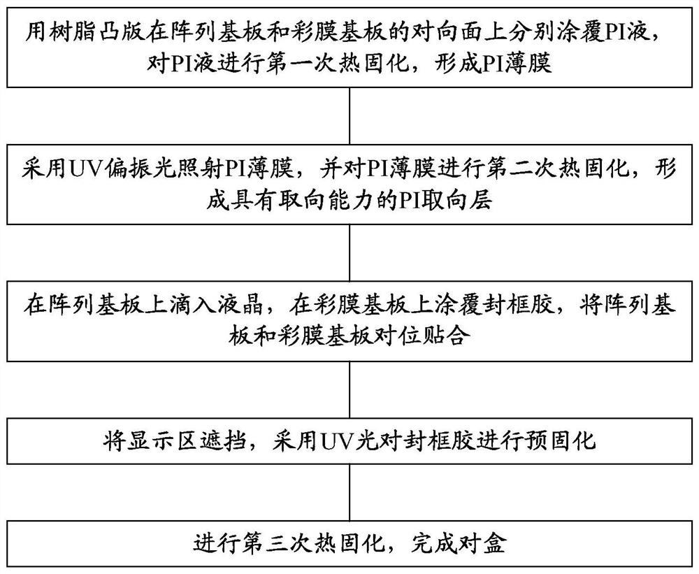
[0025] figure 1 It is a schematic flow chart of a manufacturing method of a display panel in the prior art. The main description of the process is as follows:
[0026] Use a resin letterpress to coat the PI liquid on the opposite surfaces of the array substrate and the color filter substrate, and heat-cure the PI liquid for the first time to form a PI film; irradiate the PI film with UV polarized light, and perform a second heat curing on the PI film. Secondary thermal curing to form a PI orientation layer with orientation ability; drop liquid crystal on the array substrate, coat the sealant on the color filter substrate, align and bond the array substrate and the color filter substrate; block the display area, use The UV light pre-cures the frame sealant; the third heat curing is performed to complete the box alignment.
[0027] The research of the inventors found that compared with the rubbing alignment method in the prior art display panel preparation method, the photo-al...
no. 1 example
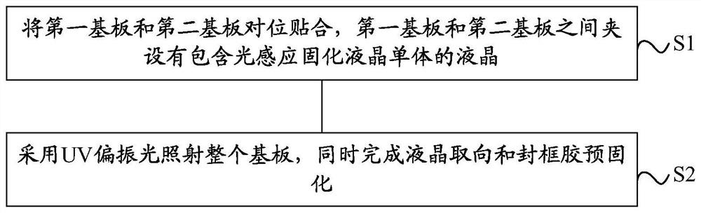
[0042] Firstly, polyimide films are respectively formed on the opposite surfaces of the first substrate and the second substrate. Specifically, it includes: coating the PI liquid on the opposite surfaces of the first substrate and the second substrate with a resin relief plate, and performing the first heat curing on the PI liquid, so as to separately coat the PI liquid on the opposite surfaces of the first substrate and the second substrate. Form PI film.
[0043] Secondly, the first substrate and the second substrate are aligned and bonded, and the liquid crystal containing the photosensitive curable liquid crystal monomer is sandwiched between the first substrate and the second substrate. It specifically includes: coating the sealant on the first substrate or the second substrate, dripping liquid crystal containing light-induced curable liquid crystal monomers on the first substrate or the second substrate; aligning the first substrate and the second substrate fit. The fr...
no. 2 example
[0049] Based on the inventive concepts of the aforementioned embodiments, the embodiments of the present invention provide a display panel, which is prepared by using the aforementioned embodiments. The display panels include Twisted Nematic (TN) type, Vertical Alignment (VA) type, In Plane Switching (IPS) and Fringe Field Switching (FFS) type display panels.
PUM
| Property | Measurement | Unit |
|---|---|---|
| wavelength | aaaaa | aaaaa |
| wavelength | aaaaa | aaaaa |
Abstract
Description
Claims
Application Information