Supercharge Your Innovation With Domain-Expert AI Agents!

Method of forming self aligned continuity blocks for mandrel and non-mandrel interconnect lines

A technology of interconnecting lines and blocks, which is applied in the manufacture of electrical components, circuits, semiconductors/solid-state devices, etc., and can solve problems such as overheating and failure

Inactive Publication Date: 2017-12-08
GLOBALFOUNDRIES INC
View PDF3 Cites 3 Cited by
  • Summary
  • Abstract
  • Description
  • Claims
  • Application Information

AI Technical Summary

Problems solved by technology

Also, a wire that is inadvertently only partially severed may still conduct for a while, but overheat and fail prematurely

Method used


Image

  • Method of forming self aligned continuity blocks for mandrel and non-mandrel interconnect lines
  • Method of forming self aligned continuity blocks for mandrel and non-mandrel interconnect lines
  • Method of forming self aligned continuity blocks for mandrel and non-mandrel interconnect lines

Examples


Embodiment Construction

[0042] Some exemplary embodiments are described at this point to provide an overall understanding of the principles of the structure, function, manufacture, and use of the methods, systems, and devices disclosed herein. One or more of these specific embodiments are illustrated in the accompanying drawings. Those skilled in the art will appreciate that the methods, systems and devices specifically described herein and illustrated in the accompanying drawings are non-limiting exemplary embodiments and that the scope of the present invention is defined solely by the claims. Features shown and described while illustrating one exemplary embodiment may be combined with features of other embodiments. Such modifications and changes are intended to be included within the scope of the present invention.

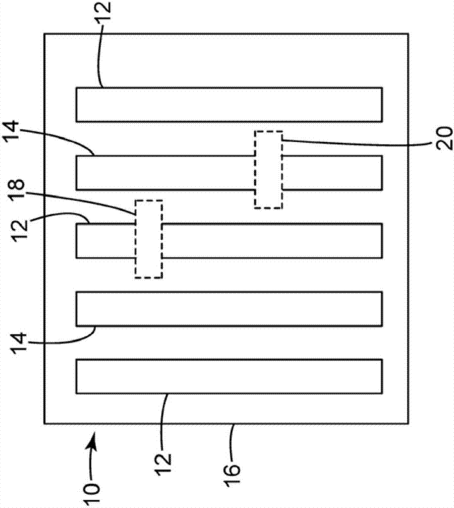
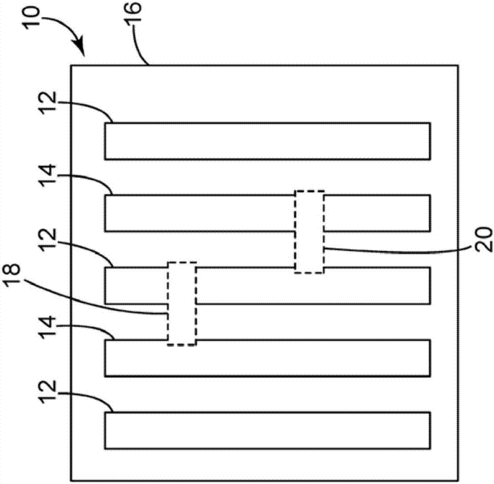
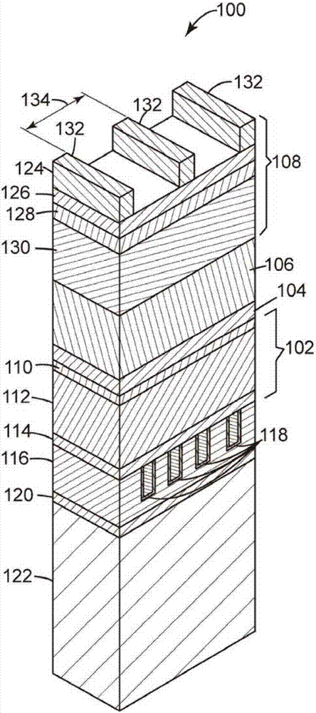
[0043] Figure 3 to Figure 16 Exemplary embodiments of various methods of forming patterns consisting of interconnect lines and associated continuity blocks for integrated circuits a...


PUM


Abstract

A method of forming a pattern for interconnect lines in an integrated circuit includes providing a structure having a first lithographic stack, a mandrel layer and a pattern layer disposed over a dielectric stack. Patterning the structure to form mandrels in the mandrel layer and disposing a spacer layer over the mandrels. Etching the spacer layer to form spacers disposed on sidewalls of the mandrels. The spacers and mandrels define beta and gamma regions. A beta region includes a beta block mask portion and a gamma region includes a gamma block mask portion of the pattern layer. The method also includes etching a beta pillar over the beta block mask portion and etching a gamma pillar over the gamma block mask portion. The method also includes etching the structure to form a pattern in the pattern layer, and the pattern includes the gamma and beta block mask portions.

Description

technical field [0001] The present invention relates to a semiconductor device and a method for manufacturing the same. More particularly, the present invention relates to various methods of patterning electrical interconnection systems in integrated circuits. Background technique [0002] With continued miniaturization and increasing demands for speed and functionality of ultra-high density integrated circuits, semiconductor devices such as transistors, diodes, capacitors, etc. require more complex and densely packed electrical interconnection systems between the devices. Conventional processes for fabricating such interconnect systems have used a series of photolithographic processes to pattern and place metal interconnect lines and vias on dielectric layers to form metallization layers. The metallization layer is disposed over the substrate in which the active semiconductor devices are buried, and the interconnection system provides contact and interconnection between th...

Claims


Application Information

Patent Timeline
Patent Type & Authority Applications(China)
IPC IPC(8): H01L21/768
CPCH01L21/76816H01L21/76838H01L21/31144H01L21/28141H10N70/068
Inventor 桂宗郁王艳汪辰辰王文辉袁磊曾嘉古拉梅·伯奇
Owner GLOBALFOUNDRIES INC
Features
  • R&D
  • Intellectual Property
  • Life Sciences
  • Materials
  • Tech Scout
  • Unparalleled Data Quality
  • Higher Quality Content
  • 60% Fewer Hallucinations
Learn More