An array substrate, its driving method and display panel

A technology for array substrates and display areas, which can be used in static indicators, instruments, nonlinear optics, etc., and can solve problems affecting the display effect of display panels

Active Publication Date: 2020-04-10
SHANGHAI TIANMA MICRO ELECTRONICS CO LTD
View PDF5 Cites 0 Cited by
  • Summary
  • Abstract
  • Description
  • Claims
  • Application Information

AI Technical Summary

Problems solved by technology

[0004] Embodiments of the present invention provide an array substrate, its driving method, and a display panel to solve the problem in the prior art that the image display effect of the display panel is affected by a large amount of residual charge

Method used


Image

  • An array substrate, its driving method and display panel
  • An array substrate, its driving method and display panel
  • An array substrate, its driving method and display panel

Examples


Embodiment Construction

[0021] In order to make the object, technical solution and advantages of the present invention more clear, the specific implementation manners of the array substrate, its driving method and the display panel provided by the embodiments of the present invention will be described in detail below with reference to the accompanying drawings.

[0022] The film thickness and shape of each layer in the drawings do not reflect the real scale of the array substrate, but are only intended to schematically illustrate the content of the present invention.

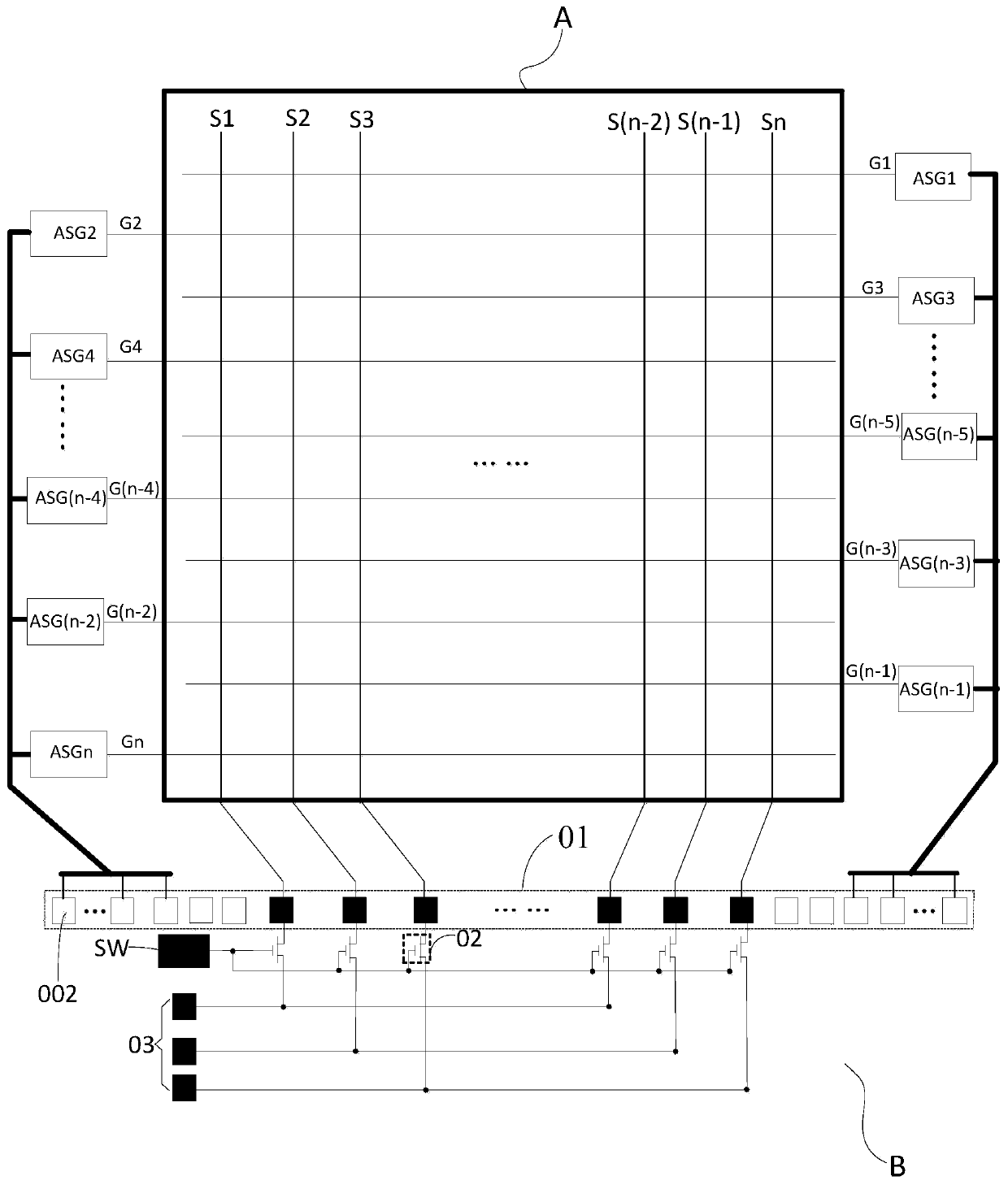
[0023] After the existing display panel is tested, a large amount of charges will remain in the data lines, which will affect the display effect of the picture. The structure of the test circuit of the existing display panel is as follows: figure 1 As shown, it includes a plurality of data lines S1, S2, S3...S(n-2), S(n-1), Sn, and a plurality of scanning lines G1, G2, G3, G4...G(n-1), Gn , a plurality of shift register units ASG1, AS...


PUM


Abstract

The invention discloses an array substrate, an array substrate driving method and a display panel. By short connection of all control ends of test switches with second-type pins in a non-display area,in a scanning stage, an integrated circuit inputs control signals to the control end of each test switch through the second-type pins to control on and off of each test switch so as to disconnect each test switch with a data line to avoid interferences on normal operations of the data line; in a scanning blank stage, the integrated circuit inputs control signals to the control end of each test switch through the second-type pins to control on and off of each test switch so as to eliminate residual electric charges in the data line. Therefore, the problem of influences on image display effectsof the display panel due to a great quantity of residual electric charges is solved, and charging efficiency improvement and power consumption reduction can be realized. On and off of each test switch can be controlled only by short connection of the control end of each test switch with the second-type pins, so that a method for eliminating the residual electric charges on the data line is simpler.

Description

technical field [0001] The present invention relates to the field of display technology, in particular to an array substrate, a driving method thereof and a display panel. Background technique [0002] During the manufacturing process of the display panel, data lines and the like need to be continuously tested to ensure the quality and performance of the display panel. An existing testing method is to form a test circuit around the array substrate while manufacturing the array substrate, test the circuit to be tested through the test circuit, and then remove the test circuit after the test is completed, and continue the subsequent manufacturing process. However, after the data line is tested and the display panel is working, since a large amount of charge remains on the data line, the display effect of the display panel will be affected. [0003] Therefore, how to eliminate the residual charge on the data line is a technical problem urgently needed to be solved by those sk...

Claims


Application Information

Patent Timeline
Patent Type & Authority Patents(China)
IPC IPC(8): G02F1/133G02F1/13
Inventor 王亚杰俞舟
Owner SHANGHAI TIANMA MICRO ELECTRONICS CO LTD
Why Eureka
Try Eureka